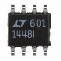
LTC1448IS8#TRPBF Linear Technology, LTC1448IS8#TRPBF Datasheet

LTC1448IS8#TRPBF
Specifications of LTC1448IS8#TRPBF
Available stocks
Related parts for LTC1448IS8#TRPBF
LTC1448IS8#TRPBF Summary of contents
Page 1
... LTC1446 data sheet.) The LTC1448 dissipates 2.5mW from a 5V supply. The low power supply current and the small SO-8 package make the LTC1448 ideal for battery-powered applications. , LTC and LT are registered trademarks of Linear Technology Corporation OUT B 8 – ...
Page 2
LTC1448 ABSOLUTE MAXIMUM V to GND .............................................. – 0.5V to 7.5V CC Logic Inputs to GND ................................ – 0. REF to GND ........... – 0. OUT A OUT B ...
Page 3
ELECTRICAL CHARACTERISTICS V = 2.7V to 5.5V, V and V unloaded, REF V CC OUT A OUT B SYMBOL PARAMETER CONDITIONS AC Performance Voltage Output Slew Rate Voltage Output Settling Time (Notes ± 0.5LSB Digital Feedthrough Reference ...
Page 4
LTC1448 W U TYPICAL PERFORMANCE CHARACTERISTICS Integral Nonlinearity (INL –1 –2 –3 –4 –5 0 2048 2560 3072 3584 4095 512 1024 1536 CODE 1448 G01 Minimum Output Voltage vs Output Sink Current 800 ...
Page 5
W BLOCK I D AGRA CLK 1 24-BIT SHIFT REGISTER CS/LD 3 REF 4 POWER-ON RESET DIAGRA S OPERATING SEQUENCE DAC A INPUT MSB D D11 D10 ...
Page 6
LTC1448 U U DEFI ITIO S Differential Nonlinearity (DNL): The differerence between the measured change and the ideal 1LSB change for any two adjacent codes. The DNL error between any two codes is calculated as follows: DNL = ( V ...
Page 7
U U APPLICATIONS INFORMATION Rail-to-Rail Output Considerations In any rail-to-rail DAC, the output swing is limited to voltages within the supply range. If the DAC offset is negative, the output for the lowest codes limits shown in ...
Page 8
LTC1448 U TYPICAL APPLICATIONS This circuit shows how to use one LTC1448 to make an autoranging ADC. The microprocessor sets the reference span and the Common pin for the analog input by loading the appropriate digital code into the LTC1448. ...
Page 9
U TYPICAL APPLICATIONS CLK CS/ PIN NOT SHOWN FOR CLARITY OUT Digitally Programmable Current Source 100V S FOR 0 REF ...
Page 10
LTC1448 PACKAGE DESCRIPTION 0.300 – 0.325 (7.620 – 8.255) 0.009 – 0.015 (0.229 – 0.381) +0.035 0.325 –0.015 +0.889 8.255 –0.381 *THESE DIMENSIONS DO NOT INCLUDE MOLD FLASH OR PROTRUSIONS. MOLD FLASH OR PROTRUSIONS SHALL NOT EXCEED 0.010 INCH (0.254mm) ...
Page 11
... FLASH SHALL NOT EXCEED 0.010" (0.254mm) PER SIDE Information furnished by Linear Technology Corporation is believed to be accurate and reliable. However, no responsibility is assumed for its use. Linear Technology Corporation makes no represen- tation that the interconnection of its circuits as described herein will not infringe on existing patent rights. ...
Page 12
... OUT Package with Clear Pin LTC1458 4.5V to 5.5V 4.095V CC OUT LTC1458L 2.7V to 5.5V 2.5V CC OUT Low Power Multiplying V DAC in MSOP-8 OUT Package. Output Swings from GND to REF. REF Input Can Be Tied 1448f LT/TP 0398 4K • PRINTED IN USA LINEAR TECHNOLOGY CORPORATION 1997 ...


