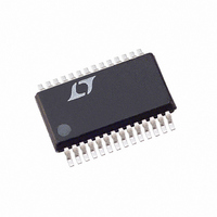
LTC1666IG#TR Linear Technology, LTC1666IG#TR Datasheet - Page 16

LTC1666IG#TR
Manufacturer Part Number
LTC1666IG#TR
Description
IC D/A CONV 12BIT 50MSPS 28-SSOP
Manufacturer
Linear Technology
Datasheet
1.LTC1668CGPBF.pdf
(24 pages)
Specifications of LTC1666IG#TR
Settling Time
20ns
Number Of Bits
12
Data Interface
Parallel
Number Of Converters
1
Voltage Supply Source
Dual ±
Power Dissipation (max)
180mW
Operating Temperature
-40°C ~ 85°C
Mounting Type
Surface Mount
Package / Case
28-SSOP
Lead Free Status / RoHS Status
Contains lead / RoHS non-compliant
Other names
LTC1666IGTR
Available stocks
Company
Part Number
Manufacturer
Quantity
Price
APPLICATIO S I FOR ATIO
LTC1666/LTC1667/LTC1668
cluding the output signal band of interest. Therefore, any
direct coupling of the digital signals to the analog output
will produce spurious tones that vary with the exact digital
input pattern.
Clock jitter should be minimized to avoid degrading the
noise floor of the device in AC applications, especially
where high output frequencies are being generated. Any
noise coupling from the digital inputs to the clock input will
cause phase modulation of the clock signal and the DAC
waveform, and can produce spurious tones. It is normally
best to place the digital data transitions near the falling
clock edge, well away from the active rising clock edge.
Because the clock signal contains spectral components
only at the sampling frequency and its multiples, it is
usually not a source of in band spurious tones. Overall, it
is better to treat the clock as you would an analog signal
and route it separately from the digital data input signals.
The clock trace should be routed either over the analog
ground plane or over its own section of the ground plane.
The clock line needs to have accurately controlled imped-
ance and should be well terminated near the LTC1666/
LTC1667/LTC1668.
Printed Circuit Board Layout Considerations—
Grounding, Bypassing and Output Signal Routing
The close proximity of high frequency digital data lines and
high dynamic range, wide-band analog signals makes
clean printed circuit board design and layout an absolute
16
SERIAL
INPUT
U
ADJUSTMENT RANGE
RELATIVE GAIN
1/2 LTC1661
U
REF
U3
5%
V
0.1 F
OUT
21k
W
Figure 9. QAM Modulation Using LTC1668 with
Digitally Controlled I vs Q Channel Gain Adjustment
2.1k
2k
0.1 F
U
REFOUT
I
REFOUT
I
REFIN
REFIN
Q-CHANNEL
I-CHANNEL
LTC1668
LTC1668
U1
U2
CLOCK
INPUT
CLK
CLK
LADCOM
LADCOM
necessity. Figures 11 to 15 are the printed circuit board
layers for an AC evaluation circuit for the LTC1668. Ground
planes should be split between digital and analog sections
as shown. All bypass capacitors should have minimum
trace length and be ceramic 0.1 F or larger with low ESR.
Bypass capacitors are required on V
and all connected to the AGND plane. The COMP2 pin ties
to a node in the output current switching circuitry, and it
requires a 0.1 F bypass capacitor. It should be bypassed
to V
should both tie directly to the AGND plane, and the tie point
between the AGND and DGND planes should nominally be
near the DGND pin. LADCOM should either be tied directly
to the AGND plane or be bypassed to AGND. The I
I
matched for good AC CMRR. The transformer output
ground should be capable of optionally being isolated or
being tied to the AGND plane, depending on which gives
better performance in the system.
Suggested Evaluation Circuit
Figure 10 is the schematic and Figures 11 to 15 are the
circuit board layouts for a suggested evaluation circuit,
DC245A. The circuit can be programmed with component
selection and jumpers for a variety of differentially coupled
transformer output and differential and single-ended re-
sistor loaded output configurations.
OUT B
I
I
I
I
OUT A
OUT B
OUT A
OUT B
SS
traces should be close together, short, and well
along with COMP1. The AGND and DGND pins
52.3
52.3
52.3
52.3
OSCILLATOR
LOW-PASS
LOW-PASS
FILTER
FILTER
LOCAL
QUADRATURE
MODULATOR
90
1666/7/8 F10
SS
, V
QAM
OUTPUT
DD
and REFOUT,
OUT A
and


