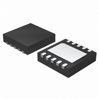
LTC2642AIDD-16#PBF Linear Technology, LTC2642AIDD-16#PBF Datasheet - Page 5

LTC2642AIDD-16#PBF
Manufacturer Part Number
LTC2642AIDD-16#PBF
Description
IC DAC 16BIT VOUT 10-DFN
Manufacturer
Linear Technology
Datasheet
1.LTC2642CDD-12PBF.pdf
(24 pages)
Specifications of LTC2642AIDD-16#PBF
Settling Time
1µs
Number Of Bits
16
Data Interface
Serial
Number Of Converters
1
Voltage Supply Source
Single Supply
Power Dissipation (max)
600µW
Operating Temperature
-40°C ~ 85°C
Mounting Type
Surface Mount
Package / Case
10-DFN
Lead Free Status / RoHS Status
Lead free / RoHS Compliant
Available stocks
Company
Part Number
Manufacturer
Quantity
Price
ELECTRICAL CHARACTERISTICS
TIMING CHARACTERISTICS
temperature range, otherwise specifi cations are at T
otherwise specified.
range, otherwise specifi cations are at T
SYMBOL
I
C
V
Power Supply
V
I
P
SYMBOL
t
t
t
t
t
t
t
t
t
f
Note 1: Stresses beyond those listed under Absolute Maximum Ratings
may cause permanent damage to the device. Exposure to any Absolute
Maximum Rating condition for extended periods may affect device
reliability and lifetime.
Note 2: Continuous operation above the specifi ed maximum operating
junction temperature may impair device reliability.
Note 3: LTC2641-16/LTC2642-16 ±1LSB = ±0.0015% = ±15.3ppm of full
scale. LTC2641-14/LTC2642-14 ±1LSB = ±0.006% = ±61ppm of full scale.
LTC2641-12/LTC2642-12 ±1LSB = ±0.024% = ±244ppm of full scale.
IN
DD
1
2
3
4
5
6
7
8
9
SCLK
IN
H
DD
D
PARAMETER
Digital Input Current
Digital Input Capacitance
Hysteresis Voltage
Supply Voltage
Supply Current, V
Power Dissipation
PARAMETER
DIN Valid to SCLK Setup Time
DIN Valid to SCLK Hold Time
SCLK Pulse Width High
SCLK Pulse Width Low
CS Pulse High Width
LSB SCLK High to CS High
CS Low to SCLK High
CS High to SCLK Positive Edge
CLR Pulse Width Low
SCLK Frequency
V
DD
High to CS Low (Power-Up Delay)
DD
A
= 25°C. V
DD
The
A
= 3V or 5V, V
= 25°C. V
l
CONDITIONS
V
(Note 6)
Digital Inputs = 0V or V
Digital Inputs = 0V or V
Digital Inputs = 0V or V
CONDITIONS
50% Duty Cycle
IN
denotes the specifi cations which apply over the full operating temperature
The
= GND to V
l
DD
denotes the specifi cations which apply over the full operating
REF
= 3V or 5V, V
DD
Note 4: R
Note 5: Reference input resistance is code dependent. Minimum is at
871Chex (34,588) in unipolar mode and at 671Chex (26, 396) in bipolar
mode.
Note 6: Guaranteed by design and not production tested.
Note 7: Guaranteed by gain error and offset error testing, not production
tested.
= 2.5V, C
DD
DD
DD
OUT
, V
, V
L
REF
= 10pF , GND = 0, R
DD
DD
tolerance is typically ±20%.
= 2.5V, C
= 5V
= 3V
L
LTC2641/LTC2642
= 10pF , GND = 0, R
l
l
l
l
l
l
l
l
l
l
l
l
l
l
L
= ∞ unless otherwise specified.
MIN
MIN
2.7
10
10
15
0
9
9
8
8
8
0.15
0.60
0.36
TYP
120
TYP
30
L
3
= ∞ unless
MAX
MAX
200
5.5
±1
10
50
UNITS
UNITS
26412fb
5
MHz
mW
mW
μA
μA
pF
ns
ns
ns
ns
ns
ns
ns
ns
ns
μs
V
V


