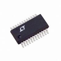
LTC1599AIG#TR Linear Technology, LTC1599AIG#TR Datasheet - Page 12

LTC1599AIG#TR
Manufacturer Part Number
LTC1599AIG#TR
Description
IC DAC 16BIT PARALLEL IN 24SSOP
Manufacturer
Linear Technology
Datasheet
1.LTC1599BCN.pdf
(20 pages)
Specifications of LTC1599AIG#TR
Settling Time
1µs
Number Of Bits
16
Data Interface
Parallel
Number Of Converters
1
Voltage Supply Source
Single Supply
Power Dissipation (max)
55µW
Operating Temperature
-40°C ~ 85°C
Mounting Type
Surface Mount
Package / Case
24-SSOP
Lead Free Status / RoHS Status
Contains lead / RoHS non-compliant
APPLICATIONS
LTC1599
Precision Voltage Reference Considerations
Much in the same way selecting an operational amplifier
for use with the LTC1599 is critical to the performance of
the system, selecting a precision voltage reference also
requires due diligence. As shown in the section describing
the basic operation of the LTC1599, the output voltage of
the DAC circuit is directly affected by the voltage reference;
thus, any voltage reference error will appear as a DAC
output voltage error.
There are three primary error sources to consider when
selecting a precision voltage reference for 16-bit applica-
tions: output voltage initial tolerance, output voltage tem-
perature coefficient and output voltage noise.
Initial reference output voltage tolerance, if uncorrected,
generates a full-scale error term. Choosing a reference
with low output voltage initial tolerance, like the LT1236
(±0.05%), minimizes the gain error caused by the refer-
ence; however, a calibration sequence that corrects for
system zero- and full-scale error is always recommended.
12
MLBYTE
U
INPUTS
CLVL
14 TO 18,
V
DATA
21 TO 23
CLR
WR
REF
LD
8
13
INFORMATION
Figure 3. Bipolar Operation (4-Quadrant Multiplication) V
U
MLBYTE
WR
R1
4
12 11
R1
LD
CLR CLVL
3
R
5
6
COM
24
R2
W
+
–
1/2 LT1112
LTC1599
10
1111
1000
1000
0111
0000
MSB
R2
IN DAC REGISTER
BINARY NUMBER
2
7
DIGITAL INPUT
1111 1111 1111
0000 0000 0001
0000 0000 0000
1111 1111 1111
0000 0000 0000
REF
Bipolar Offset Binary Code Table
U
1
V
CC
20
R
5
R
OFS
OFS
LSB
16-BIT DAC
0.1µF
5V
R
A reference’s output voltage temperature coefficient af-
fects not only the full-scale error, but can also affect the
circuit’s INL and DNL performance. If a reference is
chosen with a loose output voltage temperature coeffi-
cient, then the DAC output voltage along its transfer
characteristic will be very dependent on ambient condi-
tions. Minimizing the error due to reference temperature
coefficient can be achieved by choosing a precision refer-
ence with a low output voltage temperature coefficient
and/or tightly controlling the ambient temperature of the
circuit to minimize temperature gradients.
As precision DAC applications move to 16-bit and higher
performance, reference output voltage noise may contrib-
ute a dominant share of the system’s noise floor. This in
turn can degrade system dynamic range and signal-to-
noise ratio. Care should be exercised in selecting a voltage
reference with as low an output noise voltage as practical
for the system resolution desired. Precision voltage refer-
ences, like the LT1236, produce low output noise in the
0.1Hz to 10Hz region, well below the 16-bit LSB level in 5V
FB
V
V
0V
–V
–V
REF
REF
DGND
ANALOG OUTPUT
R
6
REF
REF
FB
(32,767/32,768)
(1/32,768)
I
OUT2S
(1/32,768)
I
OUT1
V
I
OUT2F
OUT
19
9
7
8
OUT
2
3
15pF
–
+
1/2 LT1112
= – V
REF
to V
1
REF
V
–V
OUT
REF
1599 F03
TO V
REF
sn1599 1599fs


