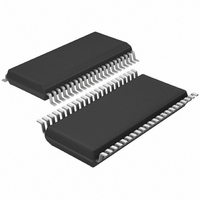
LTC2704CGW-14#PBF Linear Technology, LTC2704CGW-14#PBF Datasheet - Page 17

LTC2704CGW-14#PBF
Manufacturer Part Number
LTC2704CGW-14#PBF
Description
IC DAC 14BIT QUAD VOUT 44-SSOP
Manufacturer
Linear Technology
Datasheet
1.LTC2704IGW-12PBF.pdf
(22 pages)
Specifications of LTC2704CGW-14#PBF
Settling Time
9µs
Number Of Bits
14
Data Interface
Serial, SPI™
Number Of Converters
4
Voltage Supply Source
Analog and Digital, Dual ±
Operating Temperature
0°C ~ 70°C
Mounting Type
Surface Mount
Package / Case
44-SSOP
Lead Free Status / RoHS Status
Lead free / RoHS Compliant
Power Dissipation (max)
-
Available stocks
Company
Part Number
Manufacturer
Quantity
Price
APPLICATIONS INFORMATION
Overview
The LTC2704 is a highly integrated device, greatly sim-
plifying design and layout as compared to a design using
multiple current output DACs and separate amplifi ers. A
similar design using four separate current output DACs
would require six precision op amps, compensation capaci-
tors, bypass capacitors for each amplifi er, several times as
much PCB area and a more complicated serial interface.
Still, it is important to avoid some common mistakes in
order to achieve full performance. DC752A is the evalu-
ation board for the LTC2704. It is designed to meet all
data sheet specifi cations, and to allow the LTC2704 to be
integrated into other prototype circuitry. All force/sense
lines are available to allow the addition of current booster
stages or other output circuits.
The DC752A design is presented as a tutorial on properly
applying the LTC2704. This board shows how to properly
return digital and analog ground currents, and how to
compensate for small differences in ground potential
between the two banks of two DACs. There are other ways
to ground the LTC2704, but the one requirement is that
analog and digital grounds be connected at the LTC2704
by a very low impedance path. It is NOT advisable to split
the ground planes and connect them with a jumper or
inductor. When in doubt, use a single solid ground plane
rather than separate planes.
The LTC2704 does allow the ground potential of the DACs
to vary by ±300mV with respect to analog ground, allowing
compensation for ground return resistance.
Power Supply Grounding and Noise
LTC2704 V
output amplifi ers, ground sense amplifi ers and reference
inversion amplifi ers. These amplifi ers have good power
supply rejection, but the V
from wideband noise. The best scheme is to prefi lter low
noise regulators such as the LT
(negative). Refer to Linear Technology Application Note
101, Minimizing Switching Regulator Residue in Linear
Regulator Outputs.
+
and V
–
pins are the supplies to all of the
+
and V
®
1761 (positive) and LT1964
–
supplies must be free
The LTC2704 V
and analog DAC switches and is very sensitive to noise. It
must be treated as an analog supply. The evaluation board
uses an LT1790 precision reference as the V
minimize noise.
The GND pin is the return for digital currents and the
AGND pin is a bias point for internal analog circuitry. Both
of these pins must be tied to the same point on a quiet
ground plane.
Each DAC has a separate ground sense pin that can be used
to compensate for small differences in ground potential
within a system. Since DACs A and B are associated with
REF1 and DACs C and D are associated with REF2, the
grounds must be grouped together as follows:
AGNDA, AGNDB and REFG1 tied together (“GND1” on
DC752A)
AGNDC, AGNDD and REFG2 tied together (“GND2” on
DC752A)
This scheme allows compensation for ground return IR
drops, as long as the resistance is shared by both DACs
in a group. This implies that the ground return for DACs
A and B must be as close as possible, and GND1 must
be connected to this point through a low current, low
resistance trace. (Similar for DACs C and D.)
Figure 3 shows the top layer of the evaluation board. The
GND1 trace connects REFG1, AGNDA, AGNDB and the
ground pin of the LT1236 precision reference (U4.) This
point is the ground reference for DACs A and B. The GND2
trace connects REFG2, AGNDC, AGNDD and the ground pin
of the other LT1236 precision reference (U5). This point
is the ground reference for DACs C and D.
Voltage Reference
A high quality, low noise reference such as the LT1236
or LT1027 must be used to achieve full performance.
The ground terminal of this reference must be connected
directly to the common ground point. If GND1 and GND2
are separate, then two references must be used.
DD
pin is the supply for the digital logic
LTC2704
DD
supply to
17
2704fc


