AD7533JN Analog Devices Inc, AD7533JN Datasheet - Page 7
AD7533JN
Manufacturer Part Number
AD7533JN
Description
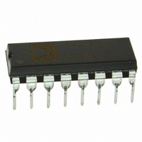
IC DAC 10BIT MULTIPLYING 16-DIP
Manufacturer
Analog Devices Inc
Datasheet
1.AD7533KRZ.pdf
(12 pages)
Specifications of AD7533JN
Data Interface
Parallel
Settling Time
600ns
Rohs Status
RoHS non-compliant
Number Of Bits
10
Number Of Converters
1
Voltage Supply Source
Single Supply
Power Dissipation (max)
30mW
Operating Temperature
-40°C ~ 85°C
Mounting Type
Through Hole
Package / Case
16-DIP (0.300", 7.62mm)
Resolution (bits)
10bit
Digital Ic Case Style
DIP
No. Of Pins
16
Operating Temperature Range
-40°C To +85°C
Update Rate
1.7MSPS
Lead Free Status / RoHS Status
Contains lead / RoHS non-compliant
Available stocks
Company
Part Number
Manufacturer
Quantity
Price
Company:

Part Number:
AD7533JN
Manufacturer:
AD
Quantity:
5 510
Part Number:
AD7533JN
Manufacturer:
ADI/亚德诺
Quantity:
20 000
Part Number:
AD7533JNZ
Manufacturer:
ADI/亚德诺
Quantity:
20 000


CIRCUIT DESCRIPTION
GENERAL CIRCUIT INFORMATION
The AD7533 is a 10-bit multiplying DAC that consists of a
highly stable thin-film R-2R ladder and ten CMOS current
switches on a monolithic chip. Most applications require the
addition of only an output operational amplifier and a voltage
or current reference.
The simplified D/A circuit is shown in Figure 7. An inverted
R- 2R ladder structure is used, that is, the binarily weighted
currents are switched between the I
thus maintaining a constant current in each ladder leg
independent of the switch state.
V
One of the CMOS current switches is shown in Figure 8. The
geometries of Device 1, Device 2, and Device 3 are optimized to
make the digital control inputs DTL/TTL/CMOS compatible
over the full military temperature range. The input stage drives
two inverters (Device 4, Device 5, Device 6, and Device 7),
which in turn drive the two output N channels. The on
resistances of the switches are binarily sealed so that the voltage
drop across each switch is the same. For example, Switch 1 in
Figure 8 is designed for an on resistance of 20 Ω, Switch 2 for
40 Ω, and so on. For a 10 V reference input, the current through
Switch 1 is 0.5 mA, the current through Switch 2 is 0.25 mA,
and so on, thus maintaining a constant 10 mV drop across each
switch. It is essential that each switch voltage drop be equal if
the binarily weighted current division property of the ladder is
to be maintained.
REF
BIT 1 (MSB)
20kΩ
S1
DIGITAL INPUTS (DTL/TTL/CMOS COMPATIBLE)
10kΩ
BIT 2
Figure 7. Functional Diagram
20kΩ
S2
10kΩ
BIT 3
20kΩ
OUT
S3
1 and I
10kΩ
BIT 10 (LSB)
OUT
20kΩ
2 bus lines,
SN
10kΩ
20kΩ
I
I
R
OUT
OUT
FB
Rev. C | Page 7 of 12
2
1
EQUIVALENT CIRCUIT ANALYSIS
The equivalent circuits for all digital inputs high and digital
inputs low are shown in Figure 9 and Figure 10. In Figure 9 with
all digital inputs low, the reference current is switched to I
The current source I
leakages to the substrate, while the I/1024 current source represents
a constant 1-bit current drain through the termination resistor
on the R-2R ladder. The on capacitance of the output N channel
switch is 100 pF, as shown on the I
capacitance is 35 pF, as shown on the I
the circuit for all digital inputs high, as shown in Figure 10, is
similar to Figure 9; however, the on switches are now on
Terminal I
DTL/TTL/
CMOS
INPUT
V
V
REF
REF
V+
I
I
REF
REF
Figure 10. Equivalent Circuit—All Digital Inputs High
250Ω
OUT
Figure 9. Equivalent Circuit—All Digital Inputs Low
1. Therefore, there is the 100 pF at that terminal.
R
R
R
10kΩ
1
LEAKAGE
I/1024
I/1024
Figure 8. CMOS Switch
R
2
10kΩ
3
is composed of surface and junction
I
I
I
I
LEAKAGE
LEAKAGE
LEAKAGE
LEAKAGE
OUT
5
4
2 terminal. The off switch
OUT
1 terminal. Analysis of
35pF
100pF
100pF
35pF
7
6
R
R
I
OUT
8
2
AD7533
R
I
I
R
I
I
TO LADDER
I
OUT
OUT
OUT
OUT
OUT
9
FB
FB
1
2
1
1
2
OUT
2.
Related parts for AD7533JN
Image
Part Number
Description
Manufacturer
Datasheet
Request
R

Part Number:
Description:
±1.7g Dual-Axis IMEMS Accelerometer Evaluation Board
Manufacturer:
Analog Devices Inc
Datasheet:

Part Number:
Description:
Inertial Sensor Evaluation System
Manufacturer:
Analog Devices Inc
Datasheet:
Part Number:
Description:
Manufacturer:
Analog Devices Inc
Datasheet:
Part Number:
Description:
Manufacturer:
Analog Devices Inc
Datasheet:
Part Number:
Description:
Manufacturer:
Analog Devices Inc
Datasheet:
Part Number:
Description:
Manufacturer:
Analog Devices Inc
Datasheet:
Part Number:
Description:
Manufacturer:
Analog Devices Inc
Datasheet:
Part Number:
Description:
Manufacturer:
Analog Devices Inc
Datasheet:
Part Number:
Description:
Manufacturer:
Analog Devices Inc
Datasheet:
Part Number:
Description:
Manufacturer:
Analog Devices Inc
Datasheet:
Part Number:
Description:
Manufacturer:
Analog Devices Inc
Datasheet:
Part Number:
Description:
Manufacturer:
Analog Devices Inc
Datasheet:
Part Number:
Description:
Manufacturer:
Analog Devices Inc
Datasheet: