AD557JP-REEL Analog Devices Inc, AD557JP-REEL Datasheet - Page 2
AD557JP-REEL
Manufacturer Part Number
AD557JP-REEL
Description
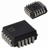
IC DAC 8BIT 5V OUT AMP 20-PLCC
Manufacturer
Analog Devices Inc
Series
DACPORT®r
Datasheet
1.AD557JNZ.pdf
(6 pages)
Specifications of AD557JP-REEL
Rohs Status
RoHS non-compliant
Settling Time
800ns
Number Of Bits
8
Data Interface
Parallel
Number Of Converters
1
Voltage Supply Source
Single Supply
Power Dissipation (max)
125mW
Operating Temperature
0°C ~ 70°C
Mounting Type
Surface Mount
Package / Case
20-PLCC
Available stocks
Company
Part Number
Manufacturer
Quantity
Price
Company:

Part Number:
AD557JP-REEL
Manufacturer:
Analog Devices Inc
Quantity:
10 000
Company:
Part Number:
AD557JP-REEL7
Manufacturer:
Analog Devices Inc
Quantity:
10 000


AD557–SPECIFICATIONS
Model
RESOLUTION
RELATIVE ACCURACY
OUTPUT
OUTPUT SETTLING TIME
FULL-SCALE ACCURACY
ZERO ERROR
MONOTONICITY
DIGITAL INPUTS
TIMING
POWER SUPPLY
POWER DISSIPATION, V
OPERATING TEMPERATURE RANGE
NOTES
1
2
3
4
5
6
Specifications shown in boldface are tested on all production units at electrical test.
Specifications subject to change without notice.
Model
AD557JN
AD557JP
Passive pull-down resistance is 2 kΩ.
Settling time is specified for a positive-going full-scale step to ± 1/2 LSB. Negative-
The full-scale output voltage is 2.55 V and is guaranteed with a 5 V supply.
A monotonic converter has a maximum differential linearity error of ± 1 LSB.
See Figure 7.
Relative Accuracy is defined as the deviation of the code transition points from the
ideal transfer point on a straight line from the offset to the full scale of the device.
See “Measuring Offset Error” on the AD558 data sheet.
going steps to zero are slower, but can be improved with an external pull-down.
0°C to 70°C
Ranges
Current Source
@ 25°C
T
@ 25°C
T
T
T
Input Current
Data Inputs, Voltage
Control Inputs, Voltage
Input Capacitance
t
t
t
Operating Voltage Range (V
W
DH
DS
MIN
MIN
MIN
MIN
Sink
Bit On—Logic “1”
Bit On—Logic “0”
On—Logic “1”
On—Logic “0”
T
T
T
2.56 Volt Range
Current (I
Rejection Ratio
Strobe Pulsewidth
Data Setup Time
MIN
Data Hold Time
MIN
MIN
to T
to T
to T
to T
6
to T
to T
to T
MAX
MAX
MAX
MAX
MAX
MAX
MAX
CC
Temperature Package
Range
0°C to 70°C
0°C to 70°C
)
5
ORDERING GUIDE
CC
4
CC
3
= 5 V
)
Description
Plastic DIP
Plastic Leaded Chip Carrier P-20A
Guaranteed But Not Tested
Min
5
2.0
0
2.0
0
225
300
10
10
225
300
4.5
0
Internal Passive
Pull-Down to Ground
Typ
± 1/2
0 to 2.56
0.8
± 1.5
± 2.5
4
15
75
(@ T
Max
8
1
1.5
± 2.5
± 4.0
± 1
± 3
0.8
0.8
5.5
25
0.03
125
70
100
A
= 25 C, V
Package
Option
N-16
2
Unit
Bits
LSB
V
mA
µs
LSB
LSB
LSB
LSB
µA
V
V
V
V
pF
ns
ns
ns
ns
ns
ns
V
mA
%/%
mW
°C
CC
= 5 V unless otherwise noted)
ABSOLUTE MAXIMUM RATINGS
V
Digital Inputs (Pins 1–10) . . . . . . . . . . . . . . . . . . . 0 V to 7.0 V
V
Power Dissipation . . . . . . . . . . . . . . . . . . . . . . . . . . . . 450 mW
Storage Temperature Range
Lead Temperature (Soldering, 10 sec) . . . . . . . . . . . . . 300°C
Thermal Resistance
nent damage to the device. This is a stress rating only; functional operation of the
device at these or any other conditions above those indicated in the operational
section of this specification is not implied. Exposure to absolute maximum rating
conditions for extended periods may affect device reliability.
Stresses above those listed under Absolute Maximum Ratings may cause perma-
CC
OUT
N/P (Plastic) Packages . . . . . . . . . . . . . . . . –25°C to +100°C
Junction to Ambient/Junction to Case
N/P (Plastic) Packages . . . . . . . . . . . . . . . . . . 140/55°C/W
to Ground . . . . . . . . . . . . . . . . . . . . . . . . . . . 0 V to 18 V
. . . . . . . . . . . . . . . . . . . . . . . Indefinite Short to Ground
NC = NO CONNECT
(MSB) BIT 1
(LSB) BIT 8
BIT 4
BIT 6
BIT 5
BIT 3
NC
PIN CONFIGURATIONS
BIT 7
BIT 6
BIT 5
BIT 4
BIT 3
BIT 2
4
5
6
7
8
1
2
3
4
5
6
7
8
9
3
(Not to Scale)
(Not to Scale)
10 11 12 13
TOP VIEW
TOP VIEW
2
PLCC
AD557
AD557
DIP
1
PIN 1
IDENTIFIER
20 19
16
15
14
13
12
11
10
9
Momentary Short to V
V
V
V
GND
GND
+V
CS
CE
18
17
16
15
14
OUT
OUT
OUT
CC
V
GND
NC
+V
GND
SENSE A
SENSE B
OUT
CC
SENSE B
CC
Related parts for AD557JP-REEL
Image
Part Number
Description
Manufacturer
Datasheet
Request
R

Part Number:
Description:
IC DAC 8BIT 5V OUT AMP 20-PLCC
Manufacturer:
Analog Devices Inc
Datasheet:
Part Number:
Description:
D/A Converter (D-A) IC
Manufacturer:
Analog Devices Inc
Datasheet:

Part Number:
Description:
DACPORT Low Cost, Complete �P-Compatible 8-Bit DAC
Manufacturer:
Analog Devices
Datasheet:

Part Number:
Description:
±1.7g Dual-Axis IMEMS Accelerometer Evaluation Board
Manufacturer:
Analog Devices Inc
Datasheet:

Part Number:
Description:
Inertial Sensor Evaluation System
Manufacturer:
Analog Devices Inc
Datasheet:
Part Number:
Description:
Manufacturer:
Analog Devices Inc
Datasheet:
Part Number:
Description:
Manufacturer:
Analog Devices Inc
Datasheet:
Part Number:
Description:
Manufacturer:
Analog Devices Inc
Datasheet:
Part Number:
Description:
Manufacturer:
Analog Devices Inc
Datasheet:
Part Number:
Description:
Manufacturer:
Analog Devices Inc
Datasheet:
Part Number:
Description:
Manufacturer:
Analog Devices Inc
Datasheet:
Part Number:
Description:
Manufacturer:
Analog Devices Inc
Datasheet:
Part Number:
Description:
Manufacturer:
Analog Devices Inc
Datasheet: