AD7533KNZ Analog Devices Inc, AD7533KNZ Datasheet - Page 6
AD7533KNZ
Manufacturer Part Number
AD7533KNZ
Description
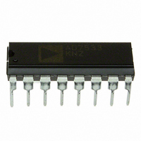
IC DAC 10BIT MULTIPLYING 16-DIP
Manufacturer
Analog Devices Inc
Datasheet
1.AD7533KRZ.pdf
(12 pages)
Specifications of AD7533KNZ
Data Interface
Parallel
Settling Time
600ns
Number Of Bits
10
Number Of Converters
1
Voltage Supply Source
Single Supply
Power Dissipation (max)
30mW
Operating Temperature
-40°C ~ 85°C
Mounting Type
Through Hole
Package / Case
16-DIP (0.300", 7.62mm)
Resolution (bits)
10bit
Sampling Rate
1.7MSPS
Input Channel Type
Parallel
Supply Voltage Range - Analogue
5V To 16V, 13.5V To 16.5V
Supply Current
2mA
Lead Free Status / RoHS Status
Lead free / RoHS Compliant
Lead Free Status / RoHS Status
Lead free / RoHS Compliant, Lead free / RoHS Compliant
Available stocks
Company
Part Number
Manufacturer
Quantity
Price
Company:

Part Number:
AD7533KNZ
Manufacturer:
Analog Devices Inc
Quantity:
135


AD7533
PIN CONFIGURATIONS AND FUNCTION DESCRIPTIONS
Table 3. Pin Function Descriptions
16-Lead PDIP, SOIC, CERDIP
1
2
3
4 to 13
14
15
16
NA
BIT 1 (MSB)
BIT 1 (MSB)
BIT 1 (MSB)
Figure 4. 16-Lead CERDIP Pin Configuration
Figure 2. 16-Lead PDIP Pin Configuration
Figure 3. 16-Lead SOIC Pin Configuration
I
I
I
I
BIT 2
BIT 3
BIT 4
BIT 5
I
I
BIT 2
BIT 3
BIT 4
BIT 5
OUT
OUT
BIT 2
BIT 3
BIT 4
BIT 5
OUT
OUT
GND
GND
OUT
OUT
GND
Pin Number
1
2
1
2
1
2
1
2
3
4
5
6
7
8
1
2
3
4
5
6
7
8
1
2
3
4
5
6
7
8
(Not to Scale)
(Not to Scale)
(Not to Scale)
AD7533
AD7533
TOP VIEW
AD7533
TOP VIEW
TOP VIEW
20-Lead LCC, PLCC
2
3
4
5, 7 to 10, 12 to 15, 17
18
19
20
1, 6, 11, 16
16
15
14
13
12
11
10
16
15
14
13
12
11
10
16
15
14
13
12
11
10
9
9
9
R
V
V
BIT 10 (LSB)
BIT 9
BIT 8
BIT 7
BIT 6
R
V
V
BIT 10 (LSB)
BIT 9
BIT 8
BIT 7
BIT 6
R
V
V
BIT 10 (LSB)
BIT 9
BIT 8
BIT 7
BIT 6
FB
REF
DD
FB
REF
DD
FB
REF
DD
Mnemonic
I
I
GND
BIT 1 to BIT 10
V
V
R
NC
OUT
OUT
DD
REF
FB
1
2
Rev. C | Page 6 of 12
Description
DAC Current Output.
DAC Analog Ground. This pin should normally be tied to the
analog ground of the system.
Ground.
MSB to LSB.
Positive Power Supply Input. These parts can be operated from
a supply of 5 V to 16 V.
DAC Reference Voltage Input Terminal.
DAC Feedback Resistor Pin. Establish voltage output for the DAC
by connecting R
No Connect.
NC = NO CONNECT
BIT 1 (MSB)
BIT 1 (MSB)
Figure 5. 20-Terminal LCC Pin Configuration
BIT 2
BIT 3
Figure 6. 20-Lead PLCC Pin Configuration
GND
FB
NC
BIT 2
BIT 3
GND
to external amplifier output.
NC
4
5
6
7
8
4
5
6
7
8
NC = NO CONNECT
3
9
3
9
(Not to scale)
(Not to Scale)
PIN 1
INDENTFIER
TOP VIEW
AD7533
10
2
AD7533
TOP VIEW
10
2
1
11
11
1
20
12
20
12
19
13
19
13
18
17
16
15
14
18
17
16
15
14
V
BIT 10 (LSB)
NC
BIT 9
BIT 8
V
BIT 10 (LSB)
NC
BIT 9
BIT 8
DD
DD
Related parts for AD7533KNZ
Image
Part Number
Description
Manufacturer
Datasheet
Request
R

Part Number:
Description:
±1.7g Dual-Axis IMEMS Accelerometer Evaluation Board
Manufacturer:
Analog Devices Inc
Datasheet:

Part Number:
Description:
Inertial Sensor Evaluation System
Manufacturer:
Analog Devices Inc
Datasheet:
Part Number:
Description:
Manufacturer:
Analog Devices Inc
Datasheet:
Part Number:
Description:
Manufacturer:
Analog Devices Inc
Datasheet:
Part Number:
Description:
Manufacturer:
Analog Devices Inc
Datasheet:
Part Number:
Description:
Manufacturer:
Analog Devices Inc
Datasheet:
Part Number:
Description:
Manufacturer:
Analog Devices Inc
Datasheet:
Part Number:
Description:
Manufacturer:
Analog Devices Inc
Datasheet:
Part Number:
Description:
Manufacturer:
Analog Devices Inc
Datasheet:
Part Number:
Description:
Manufacturer:
Analog Devices Inc
Datasheet:
Part Number:
Description:
Manufacturer:
Analog Devices Inc
Datasheet:
Part Number:
Description:
Manufacturer:
Analog Devices Inc
Datasheet:
Part Number:
Description:
Manufacturer:
Analog Devices Inc
Datasheet: