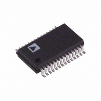
AD7805BRS Analog Devices Inc, AD7805BRS Datasheet - Page 14

AD7805BRS
Manufacturer Part Number
AD7805BRS
Description
IC DAC 10BIT QUAD PARALL 28-SSOP
Manufacturer
Analog Devices Inc
Datasheet
1.AD7808BRZ.pdf
(28 pages)
Specifications of AD7805BRS
Rohs Status
RoHS non-compliant
Settling Time
1.5µs
Number Of Bits
10
Data Interface
Parallel
Number Of Converters
4
Voltage Supply Source
Analog and Digital
Power Dissipation (max)
66mW
Operating Temperature
-40°C ~ 85°C
Mounting Type
Surface Mount
Package / Case
28-SSOP
Available stocks
Company
Part Number
Manufacturer
Quantity
Price
Company:
Part Number:
AD7805BRS
Manufacturer:
AD
Quantity:
5 510
Company:
Part Number:
AD7805BRS
Manufacturer:
INF
Quantity:
5 510
Part Number:
AD7805BRSZ
Manufacturer:
ADI/亚德诺
Quantity:
20 000
AD7804/AD7805/AD7808/AD7809
MODE
0
0
0
0
0
0
0
0
1
1
1
1
1
1
1
1
AD7805/AD7809 SYSTEM OR CHANNEL CONTROL
REGISTER SELECTION
MD0
0
1
AD7805/AD7809 SYSTEM CONTROL REGISTER
The bits in this register allow control over all DACs in the pack-
age. The control bits include data format (10/8), power down
(PD), DAC input coding select (BIN/COMP), system standby
(SSTBY) and a system clear (SCLR). The function of these bits
is as follows:
Data Format
10/8
0
1
Input Coding
BIN/COMP
0
1
Power Down
PD
0
1
System Standby
SSTBY
0
1
Table IVb. AD7809 DAC Data/Control Register
Selection Table
10-bit parallel loading structure.
Byte loading structure. (8+2 loading).
Twos complement coding.
Offset Binary Coding.
on power-up).
Complete power-down of device.
Normal operation (default on power-up).
Normal operation.
All DACs in the package put in standby mode (default
A2
0
0
0
0
1
1
1
1
0
0
0
0
1
1
1
1
This enables writing to the system control register.
The contents of this are shown in Figure 12. Mode
must be low to access this control register.
This enables writing to the channel control register.
The contents of this are shown in Figure 13. Mode
must also be low to access this control register.
A1
0
0
1
1
0
0
1
1
0
0
1
1
0
0
1
1
A0
0
1
0
1
0
1
0
1
0
1
0
1
0
1
0
1
Function Selected
DAC A Control Register
DAC B Control Register
DAC C Control Register
DAC D Control Register
DAC E Control Register
DAC F Control Register
DAC G Control Register
DAC H Control Register
DAC A Data Register
DAC B Data Register
DAC C Data Register
DAC D Data Register
DAC E Data Register
DAC F Data Register
DAC G Data Register
DAC H Data Register
–14–
System Clear
SCLR
0
1
AD7805/AD7809 CHANNEL CONTROL REGISTER
This register allows the user to have control over individual
DACs in the package. The control bits in this register include
multiplexer output selection (MX1 and MX0), Main or Sub
DAC selection (MAIN/SUB), standby (STBY) and individual
DAC clear (CLR). The function of these bits is as follows.
Multiplexer Selection (MX1, MX0)
Table V shows the V
the channel control register.
MX1
0
0
1
1
Main DAC or Sub DAC Selection
MAIN/SUB
0
1
Standby
STBY
0
1
Clear
CLR
0
1
depending on the coding scheme selected. The SCLR bit
clears the Main DACs only; the Sub DACs are unaf-
fected by the system clear function. The main DAC is
cleared to different levels depending on the coding
scheme. With offset binary coding the Main DAC output
is cleared to the bottom of the transfer function V
With twos complement coding the Main DAC output is
cleared to midscale V
sum of the Main DAC and Sub DAC contributions.
Writing a 0 to this bit means that the data in the next
data register write is transferred to the selected Main
DAC.
Writing a 1 to this bit means that the data in the next
data register write is transferred to the selected Sub DAC.
This applies to the 10-bit parallel load feature. In byte
load mode, (Figure 15) DB0 selects the Main or Sub
DAC data registers.
Places the selected DAC and its associated linear cir-
cuitry in Standby Mode.
Normal operation (default on power-up).
Normal operation.
Clears the output of the selected Main DAC to one
of two conditions depending on the input coding se-
lected. With offset binary coding the Main DAC out-
put is cleared to the bottom of the transfer function,
V
DAC output is cleared to midscale V
DAC is unaffected by a clear operation. An LDAC
signal has to be applied to the DAC for a channel clear
to be implemented.
Normal operation.
All DACs in the package are cleared to a known state
BIAS
/16 and with twos complement coding the Main
Table V. V
MX0
0
1
0
1
BIAS
selection using MX1 and MX0 bits in
BIAS
BIAS
Selection Table
V
V
INTERNAL VREF
REFIN
Undetermined
. The channel output will be the
BIAS
DD
/2 (Default on Power-Up)
BIAS
. The Sub
BIAS
REV. A
/16.


