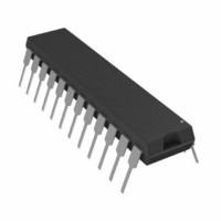
AD7845JN Analog Devices Inc, AD7845JN Datasheet - Page 4

AD7845JN
Manufacturer Part Number
AD7845JN
Description
IC DAC 12BIT MULTIPLYING 24-DIP
Manufacturer
Analog Devices Inc
Datasheet
1.AD7845JNZ.pdf
(12 pages)
Specifications of AD7845JN
Rohs Status
RoHS non-compliant
Settling Time
5µs
Number Of Bits
12
Data Interface
Parallel
Number Of Converters
1
Voltage Supply Source
Dual ±
Power Dissipation (max)
150mW
Operating Temperature
0°C ~ 70°C
Mounting Type
Through Hole
Package / Case
24-DIP (0.300", 7.62mm)
Available stocks
Company
Part Number
Manufacturer
Quantity
Price
Company:
Part Number:
AD7845JN
Manufacturer:
AD
Quantity:
6 226
Part Number:
AD7845JN
Manufacturer:
ADI/亚德诺
Quantity:
20 000
Company:
Part Number:
AD7845JNZ
Manufacturer:
ADI
Quantity:
751
AD7845
TERMINOLOGY
LEAST SIGNIFICANT BIT
This is the analog weighting of 1 bit of the digital word in a
DAC. For the AD7845, 1 LSB =
RELATIVE ACCURACY
Relative accuracy or endpoint nonlinearity is a measure of the
maximum deviation from a straight line passing through the
endpoints of the DAC transfer function. It is measured after
adjusting for both endpoints (i.e., offset and gain error are ad-
justed out) and is normally expressed in least significant bits or
as a percentage of full-scale range.
DIFFERENTIAL NONLINEARITY
Differential nonlinearity is the difference between the measured
change and the ideal 1 LSB change between any two adjacent
codes. A specified differential nonlinearity of +1 LSB max over
the operating temperature range ensures monotonicity.
GAIN ERROR
Gain error is a measure of the output error between an ideal
DAC and the actual device output with all 1s loaded after offset
error has been adjusted out. Gain error is adjustable to zero
with an external potentiometer. See Figure 13.
ZERO CODE OFFSET ERROR
This is the error present at the device output with all 0s loaded
in the DAC. It is due to the op amp input offset voltage and
bias current and the DAC leakage current.
TOTAL HARMONIC DISTORTION
This is the ratio of the root-mean-square (rms) sum of the har-
monics to the fundamental, expressed in dBs.
OUTPUT NOISE
This is the noise due to the white noise of the DAC and the
input noise of the amplifier.
DIP, SOIC
V
2
REF
12
.
PIN CONFIGURATIONS
LCC
–4–
DIGITAL-TO-ANALOG GLITCH IMPULSE
This is the amount of charge injected from the digital inputs to
the analog output when the inputs change state. This is nor-
mally specified as the area of the glitch in either pA-secs or
nV-secs depending upon whether the glitch is measured as a
current or voltage. The measurement takes place with V
AGND.
DIGITAL FEEDTHROUGH
When the DAC is not selected (i.e., CS is high) high frequency
logic activity on the device digital inputs is capacitively coupled
through the device to show up as noise on the V
noise is digital feedthrough.
MULTIPLYING FEEDTHROUGH ERROR
This is ac error due to capacitive feedthrough from the V
terminal to V
OPEN-LOOP GAIN
Open-loop gain is defined as the ratio of a change of output
voltage to the voltage applied at the V
in the DAC. It is specified at dc.
UNITY GAIN SMALL SIGNAL BANDWIDTH
This is the frequency at which the magnitude of the small signal
voltage gain of the output amplifier is 3 dB below unity. The
device is operated as a closed-loop unity gain inverter (i.e.,
DAC is loaded with all 1s).
OUTPUT RESISTANCE
This is the effective output source resistance.
FULL POWER BANDWIDTH
Full power bandwidth is specified as the maximum frequency, at
unity closed-loop gain, for which a sinusoidal input signal will
produce full output at rated load without exceeding a distortion
level of 3%.
OUT
when the DAC is loaded with all 0s.
PLCC
REF
pin with all 1s loaded
OUT
pin. This
REF
REF
REV. B
=


