AD7224LN Analog Devices Inc, AD7224LN Datasheet - Page 2
AD7224LN
Manufacturer Part Number
AD7224LN
Description
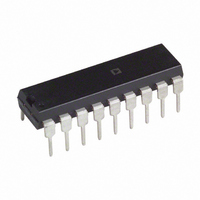
IC DAC 8BIT LC2MOS W/AMP 18-DIP
Manufacturer
Analog Devices Inc
Datasheet
1.AD7224KRZ-1.pdf
(8 pages)
Specifications of AD7224LN
Rohs Status
RoHS non-compliant
Settling Time
7µs
Number Of Bits
8
Data Interface
Parallel
Number Of Converters
1
Voltage Supply Source
Dual ±
Power Dissipation (max)
75mW
Operating Temperature
-40°C ~ 85°C
Mounting Type
Through Hole
Package / Case
18-DIP (0.300", 7.62mm)
Available stocks
Company
Part Number
Manufacturer
Quantity
Price

Company:
Part Number:
AD7224LNZ
Manufacturer:
Analog Devices Inc
Quantity:
135


DUAL SUPPLY
Parameter
STATIC PERFORMANCE
REFERENCE INPUT
DIGITAL INPUTS
DYNAMIC PERFORMANCE
POWER SUPPLIES
SWITCHING CHARACTERISTICS
NOTES
1
2
3
4
Specifications subject to change without notice.
AD7224–SPECIFICATIONS
Maximum possible reference voltage.
Temperature ranges are as follows:
K, L Versions: –40 C to +85 C
B, C Versions: –40 C to +85 C
T, U Versions: –55 C to +125 C
Sample Tested at 25 C by Product Assurance to ensure compliance.
Switching characteristics apply for single and dual supply operation.
Resolution
Total Unadjusted Error
Relative Accuracy
Differential Nonlinearity
Full-Scale Error
Full-Scale Temperature Coefficient
Zero Code Error
Zero Code Error Temperature Coefficient
Voltage Range
Input Resistance
Input Capacitance
Input High Voltage, V
Input Low Voltage, V
Input Leakage Current
Input Capacitance
Input Coding
Voltage Output Slew Rate
Voltage Output Settling Time
Digital Feedthrough
Minimum Load Resistance
V
V
I
I
t
t
t
t
t
t
1
2
3
4
5
6
DD
SS
DD
SS
Positive Full-Scale Change
Negative Full-Scale Change
@ 25 C
T
@ 25 C
T
@ 25 C
T
@ 25 C
T
@ 25 C
T
@ 25 C
T
@ 25 C
T
@ 25 C
T
Range
MIN
MIN
MIN
MIN
MIN
MIN
MIN
MIN
Range
to T
to T
to T
to T
to T
to T
to T
to T
MAX
MAX
MAX
MAX
MAX
MAX
MAX
MAX
3
3
INL
INH
(V
All specifications T
3
DD
3
= 11.4 V to 16.5 V, V
3, 4
MIN
K, B, T
Versions
8
2 to (V
8
100
2.4
0.8
8
Binary
2.5
5
7
50
2
11.4/16.5
4.5/5.5
4
6
3
5
90
90
90
90
0
0
0
0
90
90
10
10
2
1
1
3/2
20
30
50
1
to T
SS
MAX
DD
= –5 V
2
unless otherwise noted.)
– 4)
10%; AGND = DGND = O V; V
L, C, U
Versions
8
2 to (V
8
100
2.4
0.8
8
Binary
2.5
5
7
50
2
11.4/16.5
4.5/5.5
4
6
3
5
90
90
90
90
0
0
0
0
90
90
10
10
1
1/2
1
1
20
20
30
1
–2–
DD
2
– 4)
Units
Bits
LSB max
LSB max
LSB max
LSB max
ppm/ C max
mV max
V min to V max
k min
pF max
V min
V max
pF max
V/ s min
nV secs typ
k min
V min/V max
V min/V max
mA max
mA max
mA max
mA max
ns min
ns min
ns min
ns min
ns min
ns min
ns min
ns min
ns min
ns min
ns min
ns min
V/ C typ
A max
s max
s max
REF
= +2 V to (V
Conditions/Comments
V
Guaranteed Monotonic
V
Occurs when DAC is loaded with all 1s.
V
V
V
V
V
For Specified Performance
For Specified Performance
Outputs Unloaded; V
Outputs Unloaded; V
Outputs Unloaded; V
Outputs Unloaded; V
Chip Select/Load DAC Pulse Width
Write/Reset Pulse Width
Chip Select/Load DAC to Write Setup Time
Chip Select/Load DAC to Write Hold Time
Data Valid to Write Setup Time
Data Valid to Write Hold Time
DD
DD
IN
REF
REF
REF
OUT
= 0 V or V
= +15 V
= 14 V to 16.5 V, V
= +10 V; Settling Time to 1/2 LSB
= +10 V; Settling Time to 1/2 LSB
= 0 V
= +10 V
DD
– 4 V)
DD
1
5%, V
unless otherwise noted.
IN
IN
IN
IN
REF
= V
= V
= V
= V
REF
= +10 V
INL
INL
INL
INL
= +10 V
or V
or V
or V
or V
INH
INH
INH
INH
REV. B
Related parts for AD7224LN
Image
Part Number
Description
Manufacturer
Datasheet
Request
R

Part Number:
Description:
±1.7g Dual-Axis IMEMS Accelerometer Evaluation Board
Manufacturer:
Analog Devices Inc
Datasheet:

Part Number:
Description:
Inertial Sensor Evaluation System
Manufacturer:
Analog Devices Inc
Datasheet:
Part Number:
Description:
Manufacturer:
Analog Devices Inc
Datasheet:
Part Number:
Description:
Manufacturer:
Analog Devices Inc
Datasheet:
Part Number:
Description:
Manufacturer:
Analog Devices Inc
Datasheet:
Part Number:
Description:
Manufacturer:
Analog Devices Inc
Datasheet:
Part Number:
Description:
Manufacturer:
Analog Devices Inc
Datasheet:
Part Number:
Description:
Manufacturer:
Analog Devices Inc
Datasheet:
Part Number:
Description:
Manufacturer:
Analog Devices Inc
Datasheet:
Part Number:
Description:
Manufacturer:
Analog Devices Inc
Datasheet:
Part Number:
Description:
Manufacturer:
Analog Devices Inc
Datasheet:
Part Number:
Description:
Manufacturer:
Analog Devices Inc
Datasheet:
Part Number:
Description:
Manufacturer:
Analog Devices Inc
Datasheet: