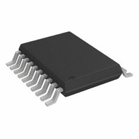
DAC8562FRU Analog Devices Inc, DAC8562FRU Datasheet - Page 6

DAC8562FRU
Manufacturer Part Number
DAC8562FRU
Description
IC DAC 12BIT PARALLEL 5V 20TSSOP
Manufacturer
Analog Devices Inc
Datasheet
1.DAC8562FSZ.pdf
(16 pages)
Specifications of DAC8562FRU
Rohs Status
RoHS non-compliant
Settling Time
16µs
Number Of Bits
12
Data Interface
Parallel
Number Of Converters
1
Voltage Supply Source
Single Supply
Power Dissipation (max)
30mW
Operating Temperature
-40°C ~ 85°C
Mounting Type
Surface Mount
Package / Case
20-TSSOP
DAC8562
As with any analog system, it is recommended that the
DAC8562 power supply be bypassed on the same PC card that
contains the chip. Figure 10 shows the power supply rejection
versus frequency performance. This should be taken into ac-
count when using higher frequency switched-mode power sup-
plies with ripple frequencies of 100 kHz and higher.
One advantage of the rail-to-rail output amplifier used in the
DAC8562 is the wide range of usable supply voltage. The part is
fully specified and tested over temperature for operation from
+4.75 V to +5.25 V. If reduced linearity and source current ca-
pability near full scale can be tolerated, operation of the
DAC8562 is possible down to +4.3 volts. The minimum operat-
ing supply voltage versus load current plot, in Figure 11, pro-
vides information for operation below V
Typical Performance Characteristics
Figure 5. Output Swing vs. Load
5
4
3
2
1
0
10
100
0%
90
10
Figure 8. Broadband Noise
50mV
100
LOAD RESISTANCE –
R
DATA = 000H
TIME = 1ms/DIV
L
TIED TO +5V
1k
RL TIED TO AGND
R
D = FFFH
DATA = FFFH
L
TIED TO AGND
V
T
DD
A
T
NBW = 630kHz
= +25
10k
A
= +5V
= 25°C
°
1ms
C
100k
DD
= +4.75 V.
0.01
100
Figure 6. Pull-Down Voltage vs.
Output Sink Current Capability
Figure 9. Supply Current vs. Logic
Input Voltage
0.1
10
1
5
4
3
2
1
0
1
0
V
DATA = 000H
T
DD
LOGIC VOLTAGE VALUE – Volts
A
= +85
= +5V
1
OUTPUT SINK CURRENT – µA
°
10
–6–
C
2
TIMING AND CONTROL
The DAC8562 has a 12-bit DAC register that simplifies inter-
face to a 12-bit (or wider) data bus. The latch is controlled by
the Chip Enable (CE) input. If the application does not involve
a data bus, wiring CE low allows direct operation of the DAC.
The data latch is level triggered and acquires data from the data
bus during the time period when CE is low. When CE goes
high, the data is latched into the register and held until CE re-
turns low. The minimum time required for the data to be
present on the bus before CE returns high is called the data
setup time (t
the amount of time that the data has to remain on the bus after
CE goes high. The high speed timing offered by the DAC8562
provides for direct interface with no wait states in all but the
fastest microprocessors.
T
A
T
= –40
A
3
= +25
100
V
T
DD
A
°
= +25
C
= +5V
°
C
4
DS
°
C
) as seen in Figure 2. The data hold time (t
1000
5
Figure 10. Power Supply Rejection
vs. Frequency
–100
100
80
60
40
20
–20
–40
–60
–80
0
80
60
40
20
0
10
Figure 7. I
1
100
OUTPUT VOLTAGE – Volts
CURRENT0
FREQUENCY – Hz
LIMIT0
POS0
V
T
DATA = FFFH
OUT
DD
A
= +25
1k
= +5V ±200mV AC
2
vs. V
NEG
CURRENT
LIMIT
°
DATA = 800H
R
C
L
TIED TO +2V
OUT
10k
REV. A
3
DH
100k
) is


