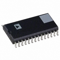
DAC8408FS Analog Devices Inc, DAC8408FS Datasheet - Page 8

DAC8408FS
Manufacturer Part Number
DAC8408FS
Description
IC DAC 8BIT QUAD W/MEMORY 28SOIC
Manufacturer
Analog Devices Inc
Datasheet
1.DAC8408FSZ-REEL.pdf
(16 pages)
Specifications of DAC8408FS
Rohs Status
RoHS non-compliant
Settling Time
190ns
Number Of Bits
8
Data Interface
Parallel
Number Of Converters
4
Voltage Supply Source
Single Supply
Operating Temperature
-40°C ~ 85°C
Mounting Type
Surface Mount
Package / Case
28-SOIC (7.5mm Width)
Power Dissipation (max)
-
Available stocks
Company
Part Number
Manufacturer
Quantity
Price
Part Number:
DAC8408FSZ
Manufacturer:
ADI/亚德诺
Quantity:
20 000
DAC8408
CIRCUIT INFORMATION
The DAC8408 combines four identical 8-bit CMOS DACs
onto a single monolithic chip. Each DAC has its own reference
input, feedback resistor, and on-board data latches. It also fea-
tures a read/write function that serves as an accessible memory
location for digital-input data words. The DAC’s three-state
readback drivers place the data word back onto the data bus.
D/A CONVERTER SECTION
Each DAC contains a highly stable, silicon-chromium, thin-film,
R-2R resistor ladder network and eight pairs of current steering
Figure 1. Simplified D/A Circuit of DAC8408
switches. These switches are in series with each ladder resistor
and are single-pole, double-throw NMOS transistors; the gates
of these transistors are controlled by CMOS inverters. Figure 1
shows a simplified circuit of the R-2R resistor ladder section,
and Figure 2 shows an approximate equivalent switch circuit.
The current through each resistor leg is switched between I
OUT 1
and I
. This maintains a constant current in each leg, re-
OUT 2
gardless of the digital input logic states.
Each transistor switch has a finite “ON” resistance that can in-
troduce errors to the DAC’s specified performance. These resis-
Figure 2. N-Channel Current Steering Switch
tances must be accounted for by making the voltage drop across
each transistor equal to each other. This is done by binarily-
scaling the transistor’s “ON” resistance from the most signifi-
cant bit (MSB) to the least significant bit (LSB). With 10 volts
applied at the reference input, the current through the MSB
switch is 0.5 mA, the next bit is 0.25 mA, etc.; this maintains a
constant 10 mV drop across each switch and the converter’s ac-
curacy is maintained. It also results in a constant resistance ap-
pearing at the DAC’s reference input terminal; this allows the
DAC to be driven by a voltage or current source, ac or dc of
positive or negative polarity.
Shown in Figure 3 is an equivalent output circuit for DAC A.
The circuit is shown with all digital inputs high. The leakage
current source is the combination of surface and junction leak-
ages to the substrate. The 1/256 current source represents the
Figure 3. Equivalent DAC Circuit (AII Digital Inputs HIGH)
constant 1-bit current drain through the ladder terminating re-
sistor. The situation is reversed with all digital inputs low, as
shown in Figure 4. The output capacitance is code dependent,
and therefore, is modulated between the low and high values.
REV. A
–8–


