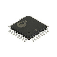
CY7C4241V-25AC Cypress Semiconductor Corp, CY7C4241V-25AC Datasheet - Page 13

CY7C4241V-25AC
Manufacturer Part Number
CY7C4241V-25AC
Description
Manufacturer
Cypress Semiconductor Corp
Datasheet
1.CY7C4241V-25AC.pdf
(18 pages)
Specifications of CY7C4241V-25AC
Configuration
Dual
Density
36Kb
Access Time (max)
15ns
Word Size
9b
Organization
4Kx9
Sync/async
Synchronous
Expandable
Yes
Bus Direction
Uni-Directional
Package Type
TQFP
Clock Freq (max)
40MHz
Operating Supply Voltage (typ)
3.3V
Operating Supply Voltage (min)
3V
Operating Supply Voltage (max)
3.6V
Supply Current
20mA
Operating Temp Range
0C to 70C
Operating Temperature Classification
Commercial
Mounting
Surface Mount
Pin Count
32
Lead Free Status / Rohs Status
Not Compliant
Available stocks
Company
Part Number
Manufacturer
Quantity
Price
Company:
Part Number:
CY7C4241V-25AC
Manufacturer:
LUCENT
Quantity:
3
Document #: 38-06010 Rev. *B
Switching Waveforms
Full Flag Timing
Programmable Almost Empty Flag Timing
Notes:
18. t
19. PAE offset = n.
20. If a read is performed on this rising edge of the read clock, there will be Empty + (n−1) words in the FIFO when PAE goes LOW.
(if applicable)
(if applicable)
WCLK and the rising RCLK is less than t
SKEW2
WEN2
WEN2
Q
D
WCLK
WEN1
REN1,
WCLK
REN1,
RCLK
WEN1
REN2
RCLK
0
0
REN2
PAE
–Q
–D
OE
is the minimum time between a rising WCLK and a rising RCLK edge for PAE to change state during that clock cycle. If the time between the edge of
FF
8
8
t
DATA IN OUTPUT REGISTER
t
LOW
SKEW1
CLKH
[11]
t
ENS
NO WRITE
(continued)
t
SKEW2
SKEW2
t
WFF
t
t
A
ENH
t
t
, then PAE may not change state until the next RCLK.
ENS
ENS
[18]
t
t
ENH
ENH
t
CLKL
NO WRITE
t
DS
t
PAE
Note 19
DATA WRITE
DATA READ
CY7C4421V/4201V/4211V/4221V
t
ENS
t
t
SKEW1
WFF
N + 1 WORDS
[11]
CY7C4231V/4241V/4251V
t
ENS
INFIFO
t
ENS
NO WRITE
t
ENH
t
WFF
t
t
A
ENH
Note 20
NEXT DATA READ
Page 13 of 18
DATA WRITE
t
PAE
[+] Feedback


