AD8582AN Analog Devices Inc, AD8582AN Datasheet
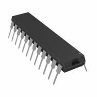
IC DAC DUAL 12BIT 5V 24-DIP

AD8582AN

Manufacturer Part Number
AD8582AN
Description
IC DAC DUAL 12BIT 5V 24-DIP
Manufacturer
Analog Devices Inc
Datasheet

Specifications of AD8582AN

Rohs Status
RoHS non-compliant
Settling Time
16µs
Number Of Bits
12
Data Interface
Parallel
Number Of Converters
2
Voltage Supply Source
Single Supply
Power Dissipation (max)
35mW
Operating Temperature
-40°C ~ 85°C
Mounting Type
Through Hole
Package / Case
24-DIP (0.300", 7.62mm)
a
GENERAL DESCRIPTION
The AD8582 is a complete, parallel input, dual 12-bit, voltage
output DAC designed to operate from a single +5 volt supply.
Built using a CBCMOS process, this monolithic DAC offers the
user low cost, and ease-of-use in +5 volt only systems.
Included on the chip, in addition to the DACs, are a rail-to-rail
amplifier, latch and reference. The reference (V
to 2.5 volts output, and the on-chip amplifier gains up the DAC
output to 4.095 volts full scale. The user needs only supply a +5
volt supply.
The AD8582 is coded natural binary. The op amp output
swings from 0 volt to +4.095 volts for a one-millivolt-per-bit
resolution, and is capable of driving 5 mA. Operation down to
4.3 V is possible with output load currents less than 1 mA.
REV. 0
Information furnished by Analog Devices is believed to be accurate and
reliable. However, no responsibility is assumed by Analog Devices for its
use, nor for any infringements of patents or other rights of third parties
which may result from its use. No license is granted by implication or
otherwise under any patent or patent rights of Analog Devices.
FEATURES
Complete Dual 12-Bit DAC
No External Components
Single +5 Volt Operation
1 mV/Bit with 4.095 V Full Scale
True Voltage Output, 5 mA Drive
Very Low Power: 5 mW
APPLICATIONS
Digitally Controlled Calibration
Portable Equipment
Servo Controls
Process Control Equipment
PC Peripherals
Figure 1. Minimum Supply Voltage vs. Load
5.0
4.8
4.6
4.4
4.2
4.0
0.01
PROPER OPERATION
DATA = FFF
T
WHEN V
VOLTAGE ABOVE
VFS
A
OUTPUT LOAD CURRENT – mA
= +25
0.1
CURVE
1 LSB
°
DD
C
SUPPLY
H
1.0
10
REF
100
) is trimmed
The high speed parallel data interface connects to the fastest
processors without wait states. The double-buffered input struc-
ture allows the user to load the input registers one at a time,
then a single load strobe tied to both LDA + LDB inputs will
update both DAC outputs simultaneously. LDA and LDB can
also be activated independently to immediately update their re-
spective DAC registers. An address input decodes DAC A or
DAC B when the chip select CS input is strobed. An asynchro-
nous reset input sets the output to zero scale. The MSB bit can
be used to establish a preset to midscale when the reset input is
strobed.
The AD8582 is available in the 24-pin plastic DIP and the sur-
face mount SOIC-24. Each part is fully specified for operation
over –40 C to +85 C, and the full +5 V
range.
Figure 2. Linearity Error vs. Digital Code and Temperature
One Technology Way, P.O. Box 9106, Norwood. MA 02062-9106, U.S.A.
Tel: 617/329-4700
DATA
LDA
LDB
A/B
CS
AD8582
Complete Dual 12-Bit DAC
–0.5
–1.0
–1.5
–2.0
FUNCTIONAL BLOCK DIAGRAM
2.0
1.5
1.0
0.5
0.0
0
DGND
12
+5 Volt, Parallel Input
DIGITAL INPUT CODE – Decimal
REGISTER
REGISTER
REGISTER
REGISTER
INPUT A
INPUT B
= +25°C & +85°C
= –55°C
1024
DAC A
DAC B
V
T
DD
A
= –55°C, +25°C, +85°C
= +5V
2048
RST
2
12
12
MSB
REFERENCE
3072
DAC A
12-BIT
12-BIT
DAC B
5% power supply
AD8582
4096
Fax: 617/326-8703
V
V
V
V
AGND
REF
DD
OUTA
OUTB

Related parts for AD8582AN

AD8582AN Summary of contents

Page 1

FEATURES Complete Dual 12-Bit DAC No External Components Single +5 Volt Operation 1 mV/Bit with 4.095 V Full Scale True Voltage Output Drive Very Low Power APPLICATIONS Digitally Controlled Calibration Portable Equipment Servo Controls Process ...

Page 2

AD8582–SPECIFICATIONS ELECTRICAL CHARACTERISTICS Parameter STATIC PERFORMANCE Resolution Relative Accuracy Differential Nonlinearity Zero-Scale Error Full-Scale Voltage Full-Scale Tempco MATCHING PERFORMANCE Linearity Matching Error REFERENCE OUTPUT Output Voltage Output Source Current Line Rejection Load Regulation ANALOG OUTPUT Output Current Load Regulation at ...

Page 3

... OUT Timing Diagram ORDERING INFORMATION* Temperature Package Model Range Description AD8582AN – +85 C 24-Pin Plastic DIP N-24 AD8582AR – +85 C 24-Lead SOIC AD8582Chips +25 C Die *For die specifications contact your local Analog Devices sales office. The AD8582 contains 1270 transistors. CAUTION ESD (electrostatic discharge) sensitive device ...

Page 4

AD8582 CS A/B LDA LDB ...

Page 5

Figures 5 and 6 in the typical performance characteristics sec- tion provide information on output swing performance near ground and full-scale as a function of load. In addition to resis- tive load driving capability, the amplifier has also been carefully ...

Page 6

AD8582–Typical Performance Characteristics +5V DD ° + TIED TO AGND L DATA = FFF TIED TO + DATA = 000 H 0 100 1k 10k ...

Page 7

V = +5V DD ° + 15µs TIME – 5µs/DIV Figure 14. Output Voltage Fall Time Detail +4.75V DD NO LOAD 298 UNITS 1 0 –1 –50 –25 ...

Page 8

AD8582 +4.75V AVG +1 0 AVG –2 –4 –6 AVG –1 –8 –10 –50 – 100 125 ° TEMPERATURE – C Figure 23. Reference Error vs. Temperature PIN ...

Related keywords