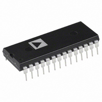
AD667KN Analog Devices Inc, AD667KN Datasheet - Page 5

AD667KN
Manufacturer Part Number
AD667KN
Description
IC DAC 12BIT W/BUFF LATCH 28-DIP
Manufacturer
Analog Devices Inc
Datasheet
1.AD667JNZ.pdf
(8 pages)
Specifications of AD667KN
Mounting Type
Through Hole
Rohs Status
RoHS non-compliant
Settling Time
3µs
Number Of Bits
12
Number Of Converters
1
Voltage Supply Source
Dual ±
Power Dissipation (max)
1W
Operating Temperature
0°C ~ 70°C
Package / Case
28-DIP (0.600", 15.24mm)
Resolution (bits)
12bit
No. Of Pins
28
Peak Reflow Compatible (260 C)
No
Update Rate
0.5MSPS
No. Of Bits
12 Bit
Leaded Process Compatible
No
Interface Type
Serial
Data Interface
-
Lead Free Status / RoHS Status
Contains lead / RoHS non-compliant
Available stocks
Company
Part Number
Manufacturer
Quantity
Price
Company:
Part Number:
AD667KN
Manufacturer:
MAXIM
Quantity:
5 510
Part Number:
AD667KN
Manufacturer:
ADI/亚德诺
Quantity:
20 000
REV. A
ANALOG CIRCUIT CONNECTIONS
Internal scaling resistors provided in the AD667 may be connected
to produce bipolar output voltage ranges of 10, 5 or 2.5 V or
unipolar output voltage ranges of 0 V to +5 V or 0 V to +10 V.
Gain and offset drift are minimized in the AD667 because of the
thermal tracking of the scaling resistors with other device com-
ponents. Connections for various output voltage ranges are
shown in Table I.
UNIPOLAR CONFIGURATION (Figure 2)
This configuration will provide a unipolar 0 volt to +10 volt out-
put range. In this mode, the bipolar offset terminal, Pin 4, should
be grounded if not used for trimming.
STEP I . . . ZERO ADJUST
Turn all bits OFF and adjust zero trimmer R1, until the output
reads 0.000 volts (1 LSB = 2.44 mV). In most cases this trim is
not needed, and Pin 4 should be connected to Pin 5.
STEP II . . . GAIN ADJUST
Turn all bits ON and adjust 100
output is 9.9976 volts. (Full scale is adjusted to 1 LSB less than
nominal full scale of 10.000 volts.)
BIPOLAR CONFIGURATION (Figure 3)
This configuration will provide a bipolar output voltage from
–5.000 to +4.9976 volts, with positive full scale occurring with
all bits ON (all 1s).
STEP I . . . OFFSET ADJUST
Turn OFF all bits. Adjust 100
volts output.
STEP II . . . GAIN ADJUST
Turn ON all bits. Adjust 100
ing of +4.9976 volts.
Figure 1. Output Amplifier Voltage Range Scaling Circuit
Figure 2. 0 V to +10 V Unipolar Voltage Output
gain trimmer R2 to give a read-
trimmer R1 to give –5.000
gain trimmer R2, until the
–5–
INTERNAL/EXTERNAL REFERENCE USE
The AD667 has an internal low noise buried Zener diode refer-
ence which is trimmed for absolute accuracy and temperature
coefficient. This reference is buffered and optimized for use in a
high speed DAC and will give long-term stability equal or superior
to the best discrete Zener reference diodes. The performance of
the AD667 is specified with the internal reference driving the
DAC since all trimming and testing (especially for full-scale
error and bipolar offset) is done in this configuration.
The internal reference has sufficient buffering to drive external
circuitry in addition to the reference currents required for the
DAC (typically 0. 5 mA to Ref In and 1.0 mA to Bipolar Off-
set). A minimum of 0.1 mA is available for driving external
loads. The AD667 reference output should be buffered with an
external op amp if it is required to supply more than 0.1 mA
output current. The reference is typically trimmed to 0.2%,
then tested and guaranteed to 1.0% max error. The tempera-
ture coefficient is comparable to that of the full-scale TC for a
particular grade.
If an external reference is used (10.000 V, for example), addi-
tional trim range must be provided, since the internal reference
has a tolerance of 1%, and the AD667 full-scale and bipolar
offset are both trimmed with the internal reference. The gain
and offset trim resistors give about 0.25% adjustment range,
which is sufficient for the AD667 when used with the internal
reference.
It is also possible to use external references other than 10 volts.
The recommended range of reference voltage is from +8 to
+11 volts, which allows both 8.192 V and 10.24 V ranges to be
used. The AD667 is optimized for fixed-reference applications.
If the reference voltage is expected to vary over a wide range in a
particular application, a CMOS multiplying DAC is a better
choice.
Reduced values of reference voltage will also permit the
volt
It is not recommended that the AD667 be used with external
feedback resistors to modify the scale factor. The internal resis-
tors are trimmed to ratio-match and temperature-track the other
resistors on the chip, even though their absolute tolerances are
–50 ppm/ C. If external resistors are used, a wide trim range
( 20%) will be needed and temperature drift will be increased
to reflect the mismatch between the temperature coefficients of
the internal and external resistors.
20%, and absolute temperature coefficients are approximately
10%.
5% power supply requirement to be relaxed to 12 volts
Figure 3.
5 V Bipolar Voltage Output
AD667
12


