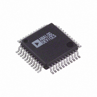
AD7836ASZ Analog Devices Inc, AD7836ASZ Datasheet - Page 5

AD7836ASZ
Manufacturer Part Number
AD7836ASZ
Description
IC DAC 14BIT QUAD LC2MOS 44MQFP
Manufacturer
Analog Devices Inc
Datasheet
1.AD7836ASZ.pdf
(12 pages)
Specifications of AD7836ASZ
Data Interface
Parallel
Settling Time
16µs
Number Of Bits
14
Number Of Converters
4
Voltage Supply Source
Analog and Digital, Dual ±
Power Dissipation (max)
460mW
Operating Temperature
-40°C ~ 85°C
Mounting Type
Surface Mount
Package / Case
44-MQFP, 44-PQFP
Resolution (bits)
14bit
Sampling Rate
62.5kSPS
Input Channel Type
Parallel
Supply Current
7mA
Digital Ic Case Style
QFP
No. Of Pins
44
Lead Free Status / RoHS Status
Lead free / RoHS Compliant
Available stocks
Company
Part Number
Manufacturer
Quantity
Price
Company:
Part Number:
AD7836ASZ
Manufacturer:
ADI
Quantity:
183
Company:
Part Number:
AD7836ASZ
Manufacturer:
Analog Devices Inc
Quantity:
10 000
Part Number:
AD7836ASZ
Manufacturer:
ADI/亚德诺
Quantity:
20 000
REV. A
Pin Mnemonic
V
V
V
DGND
AGND
V
V
V
V
V
CS
DB0 . . . DB13
A0, A1, A2
CLR
WR
DUTGND A
DUTGND B
DUTGND C
DUTGND D
SEL
CC
SS
DD
REF
REF
REF
REF
OUT
(+)A, V
(+)B, V
(+)C, V
(+)D, V
A . . . V
REF
REF
REF
OUT
REF
(–)B
(–)A
(–)C
(–)D
D
Description
Logic Power Supply; +5 V ± 5%.
Negative Analog Power Supply; –15 V ± 5%.
Positive Analog Power Supply; +15 V ± 5%.
Digital Ground.
Analog Ground.
Reference Inputs for DAC A. These reference voltages are referred to AGND.
Reference Inputs for DAC B. These reference voltages are referred to AGND.
Reference Inputs for DAC C. These reference voltages are referred to AGND.
Reference Inputs for DAC D. These reference voltages are referred to AGND.
DAC Outputs.
Level-Triggered Chip Select Input (active low). The device is selected when this input is low.
Parallel Data Inputs. The AD7836 can accept a straight 14-bit parallel word on DB0 to DB13 where
DB13 is the MSB and DB0 is the LSB.
Address inputs. A0, A1 and A2 are decoded to select one of the five input latches for a data transfer.
Asynchronous Clear Input (level sensitive, active low). When this input is low, all analog outputs are
switched to the externally set potential on the DUTGND pin. The contents of data registers A to E are
not affected when the CLR pin is taken low. When CLR is brought back high, the DAC outputs revert
back to their original outputs as determined by the data in their data registers.
Level-Triggered Write Input (active low), when active and used in conjunction with CS to write data to
the AD7836 input buffer. Data is latched into the selected data register on the rising edge of WR.
Device Sense Ground for DAC A. Vout A is referenced to the voltage applied to this pin.
Device Sense Ground for DAC B. Vout B is referenced to the voltage applied to this pin.
Device Sense Ground for DAC C. Vout C is referenced to the voltage applied to this pin.
Device Sense Ground for DAC D. Vout D is referenced to the voltage applied to this pin.
Select pin, active high level triggered input. When the SEL input is high, the user programmed value in
DATAREG E will be loaded into all DAC registers and the DAC outputs updated accordingly. The con-
tents of the other DATA REGs (A–D) will not be affected by the SEL pin.
NC = NO CONNECT
V
V
V
V
REF
REF
REF
REF
V
V
AGND
OUT
OUT
(–)C
(+)C
V
(+)A
(–)A
V
NC
NC
DD
SS
C
A
34
35
36
37
38
39
40
41
42
43
44
33
1
PIN CONFIGURATION
32
PIN 1
IDENTIFIER
2
PIN DESCRIPTION
31
3
30
4
(Not to Scale)
29
5
–5–
TOP VIEW
AD7836
28
6
27
7
26
8
25
9 10 11
24
23
22
19
18
17
16
15
14
13
21
20
12
DB7
DB6
DB5
DB4
DB3
DB2
DB1
DB0
DGND
V
CLR
CC
AD7836


