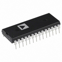
AD7846KNZ Analog Devices Inc, AD7846KNZ Datasheet - Page 5

AD7846KNZ
Manufacturer Part Number
AD7846KNZ
Description
IC DAC 16BIT LC2MOS VOUT 28-DIP
Manufacturer
Analog Devices Inc
Datasheet
1.AD7846JPZ.pdf
(24 pages)
Specifications of AD7846KNZ
Data Interface
Parallel
Settling Time
7µs
Number Of Bits
16
Number Of Converters
1
Voltage Supply Source
Dual ±
Power Dissipation (max)
100mW
Operating Temperature
0°C ~ 70°C
Mounting Type
Through Hole
Package / Case
28-DIP (0.600", 15.24mm)
Resolution (bits)
16bit
Sampling Rate
143kSPS
Input Channel Type
Parallel
Supply Voltage Range - Digital
4.75V To 5.25V
Supply Current
5mA
Digital Ic Case Style
DIP
Lead Free Status / RoHS Status
Lead free / RoHS Compliant
Available stocks
Company
Part Number
Manufacturer
Quantity
Price
Part Number:
AD7846KNZ
Manufacturer:
ADI/亚德诺
Quantity:
20 000
TIMING CHARACTERISTICS
V
Table 3.
Parameter
t
t
t
t
t
t
t
t
t
t
t
t
1
2
3
1
2
3
4
5
6
7
8
9
10
11
12
Timing specifications are sample tested at +25°C to ensure compliance. All input control signals are specified with t
voltage level of 1.6 V.
t
t
2
3
6
7
DD
is measured with the load circuits of Figure 3 and Figure 4 and defined as the time required for an output to cross 0.8 V or 2.4 V.
is defined as the time required for an output to change 0.5 V when loaded with the circuits of Figure 5 and Figure 6.
= +14.25 V to +15.75 V, V
Figure 4. Load Circuits for Bus Relinquish Time (t
Figure 3. Load Circuit for Access Time (t
1
DBn
Limit at T
0
60
0
60
0
120
10
60
0
70
0
70
130
DBn
3kΩ
DGND
SS
MIN
5V
= −14.25 V to −15.75 V, V
3kΩ
100pF
DGND
to T
LDAC
DB15
DB0
CLR
MAX
R/W
CS
100pF
TO
6
)—High Z to V
(All Versions)
6
)—High Z to V
t
1
t
8
DATA VALID
t
OH
4
t
t
2
9
OL
Figure 2. Timing Diagram
CC
Rev. G | Page 5 of 24
= +4.75 V to +5.25 V, unless otherwise noted.
t
t
5
10
t
3
t
1
t
8
Unit
ns min
ns min
ns min
ns min
ns min
ns max
ns min
ns max
ns min
ns min
ns min
ns min
ns min
t
6
t
12
t
DATA VALID
9
Figure 6. Load Circuits for Bus Relinquish Time (t
Figure 5. Load Circuit for Access Time (t
t
10
t
3
t
7
DBn
t
11
R
= t
5V
0V
5V
0V
5V
0V
5V
0V
5V
0V
DBn
F
Test Conditions/Comments
R/W to CS setup time
CS pulse width (write cycle)
R/W to CS hold time
Data setup time
Data hold time
Data access time
Bus relinquish time
CLR setup time
CLR pulse width
CLR hold time
LDAC pulse width
CS pulse width (read cycle)
= 5 ns (10% to 90% of +5 V) and timed from a
3kΩ
DGND
5V
3kΩ
10pF
DGND
10pF
7
)—High Z to V
7
)—High Z to V
AD7846
OH
OL


