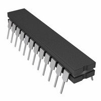
AD660SQ Analog Devices Inc, AD660SQ Datasheet

AD660SQ
Specifications of AD660SQ
Available stocks
Related parts for AD660SQ
AD660SQ Summary of contents
Page 1
... REF OUT EE CC Figure 1. is also available compliant to MIL-STD-883. Refer to the AD660SQ/883B military data sheet for specifications and test conditions. PRODUCT HIGHLIGHTS 1. The AD660 is a complete 16-bit DAC, with a voltage reference, double-buffered latches, and an output amplifier on a single chip. 2. The internal buried Zener reference is laser trimmed to 10.000 V with a ± ...
Page 2
AD660 TABLE OF CONTENTS Features .............................................................................................. 1 Functional Block Diagram .............................................................. 1 General Description ......................................................................... 1 Product Highlights ........................................................................... 1 Revision History ............................................................................... 2 Specifications ..................................................................................... 3 AC Performance Characteristics ................................................ 4 Timing Characteristics ................................................................ 5 Absolute Maximum Ratings ............................................................ ...
Page 3
SPECIFICATIONS T = 25° −V = − Table 1. Parameter RESOLUTION DIGITAL INPUTS ( MIN MAX V (Logic (Logic 5.5 ...
Page 4
AD660 Parameter POWER SUPPLIES Voltage − Current (No Load 2 ...
Page 5
TIMING CHARACTERISTICS + −V = − Table 3. Parameter BYTE LOAD (see Figure BES t BEH ...
Page 6
AD660 DB0 t SS SER DB1 1 = MSB FIRST LSB FIRST (DATADIR) CS LDAC CLR LBE DB0 SER DB1 (DATADIR OUT VALID 1 VALID LOW HIGH t CLK ...
Page 7
ABSOLUTE MAXIMUM RATINGS Table 4. Parameter Rating +V to AGND −0 +17 −V to AGND +0 −17 DGND −0 AGND to DGND ±1 V Digital ...
Page 8
AD660 PIN CONFIGURATION AND FUNCTION DESCRIPTIONS Table 5. Pin Function Descriptions Pin No. Mnemonic Description 1 −V Negative Analog Supply Pin Positive Analog Supply Pin Digital Supply Pin LL 4 DGND Digital Ground Reference ...
Page 9
TERMINOLOGY Integral Nonlinearity Integral nonlinearity is the maximum deviation of the actual, adjusted DAC output from the ideal analog output (a straight line drawn from − 1 LSB) for any bit combination. This is also referred to ...
Page 10
AD660 THEORY OF OPERATION The AD660 uses an array of bipolar current sources with MOS current steering switches to develop a current proportional to the applied digital word, ranging from mA. A segmented architecture is used, ...
Page 11
BIPOLAR CONFIGURATION The circuit shown in Figure 10 provides a bipolar output voltage from −10.000000 V to +9.999694 V with positive full scale occur- ring with all bits on the unipolar mode, Resistor R1 and Resistor R2 can ...
Page 12
AD660 It is also possible to use external references other than 10 V with slightly degraded linearity specifications. The recommended range of reference voltages 10.24 V, which allows 5 V, 8.192 V, and 10.24 V ranges ...
Page 13
AD688 Figure 13. Using the AD660 with the AD688 High Precision ±10 V Reference OUTPUT SETTLING AND GLITCH The ...
Page 14
AD660 DIGITAL CIRCUIT DETAILS The AD660 has several dual-use pins that allow flexible opera- tion while maintaining the lowest possible pin count and consequently the smallest package size. The user should, therefore, pay careful attention to the following information when ...
Page 15
MICROPROCESSOR INTERFACE AD660 TO MC68HC11 (SPI BUS) INTERFACE The AD660 interface to the Motorola SPI (serial peripheral interface) is shown in Figure 17. The MOSI, SCK, and SS pins of the 68HC11 are respectively connected to the DB0/DB8/SIN ...
Page 16
AD660 In applications such as waveform generation, accurate timing of the output samples is important to avoid noise that is induced by jitter on the LDAC signal. In this example, the ADSP-210x is set up to use the internal timer ...
Page 17
BOARD LAYOUT Designing with high resolution data converters requires careful attention to board layout. Trace impedance is the first issue. A 306 μA current through a 0.5 Ω trace develops a voltage drop of 153 μV, which is 1 LSB ...
Page 18
AD660 OUTLINE DIMENSIONS 24 0.210 (5.33) MAX 0.150 (3.81) 0.130 (3.30) 0.115 (2.92) 0.022 (0.56) 0.018 (0.46) 0.014 (0.36) CONTROLLING DIMENSIONS ARE IN INCHES; MILLIMETER DIMENSIONS (IN PARENTHESES) ARE ROUNDED-OFF INCH EQUIVALENTS FOR REFERENCE ONLY AND ARE NOT APPROPRIATE FOR ...
Page 19
... AD660BRZ-REEL −40°C to +85°C AD660SQ −55°C to +125°C 2 AD660SQ/883B −55°C to +125° RoHS Compliant Part. 2 For further details, refer to the AD660SQ/883B military data sheet. 15.60 (0.6142) 15.20 (0.5984 7.60 (0.2992) 7.40 (0.2913) 1 10.65 (0.4193) 12 10.00 (0.3937) 2.65 (0.1043) 2 ...
Page 20
AD660 NOTES ©1993–2008 Analog Devices, Inc. All rights reserved. Trademarks and registered trademarks are the property of their respective owners. D01813-0-6/08(B) Rev Page ...


