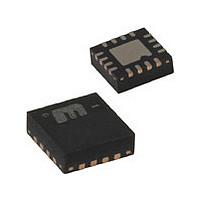
SY89871UMITR Micrel Inc, SY89871UMITR Datasheet

SY89871UMITR
Specifications of SY89871UMITR
Related parts for SY89871UMITR
SY89871UMITR Summary of contents
Page 1
Micrel, Inc. FEATURES Two matched-delay outputs: • Bank A: undivided pass-through (QA) • Bank B: programmable divide (QB0, QB1) Matched delay: all outputs have matched delay, independent of divider setting Guaranteed AC performance: • >2.5GHz ...
Page 2
... X X M9999-082407 hbwhelp@micrel.com or (408) 955-1690 Ordering Information Package Operating Part Number Type SY89871UMI MLF-16 (1) SY89871UMITR MLF-16 (2) SY89871UMG MLF-16 (1, 2) SY89871UMGTR MLF-16 Notes: 1. Contact factory for die availability. Dice are guaranteed Tape and Reel. 3. Pb-Free package is recommended for new designs. Pin Function Differential Buffered Output Clocks: This differential output is a divided-down version of the input frequency and has a matched output delay with Bank A. Divided 16. See “ ...
Page 3
Micrel, Inc. Absolute Maximum Ratings Supply Voltage (V ) ................................... –0.5V to +4.0V CC Input Voltage (V ) ............................... –0. PECL Output Current (I ) OUT Continuous .......................................................... 50mA Surge .................................................................100mA V Current (I ) ...................................................... ±100mA ...
Page 4
Micrel, Inc. (100KEP) LVPECL DC ELECTRICAL CHARACTERISTICS V = 3.3V ±10% or 2.5V ±5 –40°C to +85° Symbol Parameter V Output HIGH Voltage OH V Output LOW Voltage OL V Output Voltage Swing OUT V ...
Page 5
Micrel, Inc. AC ELECTRICAL CHARACTERISTICS V = 3.3V ±10% or 2.5V ±5 –40°C to +85°C, unless otherwise stated Symbol Parameter f Maximum Output Toggle Frequency MAX Maximum Input Frequency t Differential Propagation Delay PD IN-to-QA or ...
Page 6
Micrel, Inc. TYPICAL OPERATING CHARACTERISTICS V = 3.3V 400mV 25° 50ý Output Amplitude vs. Frequency 900 800 700 600 500 400 300 200 100 0 FREQUENCY (MHz) ...
Page 7
Micrel, Inc. DEFINITION OF SINGLE-ENDED AND DIFFERENTIAL SWING Figure 1a. Single-Ended Swing INPUT BUFFER STRUCTURE V CC 1.86kΩ 1.86kΩ IN 50Ω 50Ω GND /IN Figure 2a. Simplified Differential Input Buffer M9999-082407 hbwhelp@micrel.com or (408) 955-1690 V V IN, ...
Page 8
Micrel, Inc. INPUT INTERFACE APPLICATIONS CML /IN SY89871U GND REF-AC Figure 3a. DC-Coupled CML Input Interface PECL / SY89871U ...
Page 9
Micrel, Inc. LVPECL OUTPUT TERMINATION RECOMMENDATIONS Figure 4a. Parallel Termination–Thevenin Equivalent Note: 1. For +2.5V systems 250ý 62.5ý. Notes: 1. Power-saving alternative to Thevenin termination. 2. Place termination resistors as close to destination inputs as possible. ...
Page 10
Micrel, Inc. ® 16-PIN MicroLeadFrame Package Notes: 1. Package meets Level 2 moisture sensitivity classification, and is shipped in dry-pack form. 2. Exposed pads must be soldered to a ground for proper thermal management. MICREL, INC. 2180 FORTUNE DRIVE SAN ...


