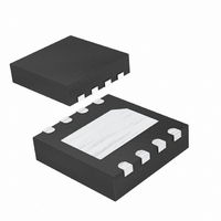
MAX5547ETA+T Maxim Integrated Products, MAX5547ETA+T Datasheet

MAX5547ETA+T
Specifications of MAX5547ETA+T
Related parts for MAX5547ETA+T
MAX5547ETA+T Summary of contents
Page 1
... GND I/O1 TX_DISABLE MOD-DEF1 MOD-DEF2 SPI is a trademark of Motorola, Inc. ________________________________________________________________ Maxim Integrated Products For pricing, delivery, and ordering information, please contact Maxim Direct at 1-888-629-4642, or visit Maxim’s website at www.maxim-ic.com. o Dual Current-Sink DACs o 10-Bit Resolution o Two Software-Programmable Full-Scale Current Ranges: 3.6mA or 1.2mA o Parallelable Outputs for Up to 7.2mA (max) o +2.5V Internal Reference Drifts Only 4ppm/° ...
Page 2
Dual, 10-Bit, Current-Sink Output DAC ABSOLUTE MAXIMUM RATINGS V to GND .............................................................-0.3V to +6V DD OUTA, OUTB, REF to GND ........................-0. SCLK, DIN GND ............................................-0.3V to +6V Continuous Power Dissipation (T = +70°C) A 8-Pin TDFN ...
Page 3
Dual, 10-Bit, Current-Sink Output DAC ELECTRICAL CHARACTERISTICS (continued +2.7V to +5.25V 0V, external reference = +2.5V, output voltage = +2.0V GND V = +3.0V, and T = +25°C.) (Note PARAMETER SYMBOL ...
Page 4
Dual, 10-Bit, Current-Sink Output DAC ELECTRICAL CHARACTERISTICS (continued +2.7V to +5.25V 0V, external reference = +2.5V, output voltage = +2.0V GND V = +3.0V, and T = +25°C.) (Note PARAMETER SYMBOL ...
Page 5
Dual, 10-Bit, Current-Sink Output DAC (V = +3.0V 0V, external reference = +2.5V GND DIFFERENTIAL NONLINEARITY vs. DIGITAL INPUT CODE (3.6mA SETTING) 1.00 0.75 0.50 0.25 0 -0.25 -0.50 -0.75 -1.00 0 256 512 768 DIGITAL ...
Page 6
Dual, 10-Bit, Current-Sink Output DAC (V = +3.0V 0V, external reference = +2.5V GND SUPPLY CURRENT vs. SUPPLY VOLTAGE 1.12 INTERNAL REFERENCE SCLK = DIN = GND 1.11 1.10 1.09 1.08 2.5 3.0 3.5 ...
Page 7
Dual, 10-Bit, Current-Sink Output DAC (V = +3.0V 0V, external reference = +2.5V GND SETTLING TIME (FULL-SCALE NEGATIVE STEP 3.6mA) OUT_ MAX5547 toc22 SCLK 2V/div 15 16 GND 3V OUT_ 500mV/div V = 3V, ...
Page 8
Dual, 10-Bit, Current-Sink Output DAC PIN NAME Supply Voltage. Set the device as possible. CS Active-Low Chip-Select Input. Set CS low to enable the serial interface SCLK Serial-Clock Input 4 DIN Serial-Data Input. DIN ...
Page 9
Dual, 10-Bit, Current-Sink Output DAC CSS CL CH SCLK DIN C3 Figure 1. SPI Serial-Interface Timing Diagram Set CS low to begin clocking input data at DIN on the falling edge of ...
Page 10
Dual, 10-Bit, Current-Sink Output DAC Table 1. Command Word Summary MSB CONTROL BITS ...
Page 11
Dual, 10-Bit, Current-Sink Output DAC +2.5V REF +2.5V REFERENCE SERIAL INTERFACE CS DIN Chip Information PROCESS: BiCMOS ______________________________________________________________________________________ +2.7V TO +5.25V V DD DAC A DAC REGISTER A RANGE CONTROL DACB DAC REGISTER B RANGE CONTROL GND SCLK For the ...
Page 12
... Maxim cannot assume responsibility for use of any circuitry other than circuitry entirely embodied in a Maxim product. No circuit patent licenses are implied. Maxim reserves the right to change the circuitry and specifications without notice at any time. 12 ____________________Maxim Integrated Products, 120 San Gabriel Drive, Sunnyvale, CA 94086 408-737-7600 © 2009 Maxim Integrated Products DESCRIPTION and linearity information ...


