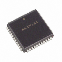
MAX547BCQH+D Maxim Integrated Products, MAX547BCQH+D Datasheet - Page 8

MAX547BCQH+D
Manufacturer Part Number
MAX547BCQH+D
Description
IC DAC OCTL V-OUT 13BIT 44-PLCC
Manufacturer
Maxim Integrated Products
Datasheet
1.MAX547BCQH-D.pdf
(16 pages)
Specifications of MAX547BCQH+D
Settling Time
5µs
Number Of Bits
13
Data Interface
Parallel
Number Of Converters
8
Voltage Supply Source
Dual ±
Power Dissipation (max)
1.07W
Operating Temperature
0°C ~ 70°C
Mounting Type
Surface Mount
Package / Case
44-LCC, 44-PLCC
Resolution
13 bit
Interface Type
Parallel
Maximum Operating Temperature
+ 70 C
Mounting Style
SMD/SMT
Minimum Operating Temperature
0 C
Lead Free Status / RoHS Status
Lead free / RoHS Compliant
Octal, 13-Bit Voltage-Output
DAC with Parallel Interface
The REF_ inputs can range between AGND_ and V
However, the DAC outputs will operate to V
and V
swing limitations. The AGND_ inputs can be offset by
any voltage within the supply rails. The offset-voltage
potential must be lower than the reference-voltage
potential. For more information, refer to the Digital Code
and Analog Output Voltage section in the Applications
Information.
The input impedance of the REF_ inputs is code depen-
dent. It is at its lowest value (5kΩ min) when the input
code of the referring DAC pair is 0 1010 1010 1010
(0AAAhex). Its maximum value, typically 50kΩ, occurs
when the code is 0000hex. When all reference inputs are
driven from the same source, the minimum load imped-
ance is 1.25kΩ. Since the input impedance at REF_ is
code dependent, load regulation of the reference used is
important. For more information, see Reference
Selection in the Applications Information section.
The input capacitance at REF_ is also code dependent,
and typically varies from 125pF to 300pF. Its minimum
value occurs when the code of the referring DAC pair is
set to all 0s. It is at its maximum value with all 1s on both
DACs.
The MAX547’s voltage outputs are internally buffered
by precision gain-of-two amplifiers with a typical slew
rate of 3V/µs. With a full-scale transition at its output,
the typical settling time to ±
with 10kΩ in parallel with 50pF, or 6µs when loaded
with 10kΩ in parallel with 100pF.
All digital inputs are compatible with both TTL and
CMOS logic. The MAX547 interfaces with microproces-
sors using a data bus at least 13 bits wide. The inter-
face is double buffered, allowing simultaneous update
of all DACs. There are two latches for each DAC (see
Functional Diagram ): an input latch that receives data
from the data bus, and a DAC latch that receives data
from the input latch. Address lines A0, A1, and A2
select which DAC’s input latch receives data from the
data bus, as shown in Table 1. Transfer data from the
input latches to the DAC latches by asserting the asyn-
chronous LD_ signal. Each DAC’s analog output
reflects the data held in its DAC latch. All control inputs
are level triggered.
Data can be latched or transferred directly to the DAC.
CS and WR control the input latch and LD_ transfers
information from the input latch to the DAC latch. The
input latch is transparent when CS and WR are low, and
8
_______________________________________________________________________________________
SS
+ 0.6V, due to the output amplifiers’ voltage-
Digital Inputs and Interface Logic
Reference and Analog-Ground Inputs
1
⁄
Output Buffer Amplifiers
2
LSB is 5µs when loaded
DD
- 0.6V
DD
.
the DAC latch is transparent when LD_ is low. The
address lines (A0, A1, A2) must be valid throughout the
time CS and WR are low (Figure 3). Otherwise, the data
can be inadvertently written to the wrong DAC. Data is
latched within the input latch when either CS or WR is
high. Taking LD_ high latches data into the DAC latches.
If LD_ is brought low when WR and CS are low, it must
be held low for t
(Figure 3).
Pulling the asynchronous CLR input low sets all DAC
outputs to a nominal 0V, regardless of the state of CS,
WR, and LD_. Taking CLR high latches 1000hex into
all input latches and DAC latches.
Figure 2. Input Control Logic
Table 1. MAX547 DAC Addressing
LDGH
LDCD
LDAB
A2
LDEF
CLR
0
0
0
0
1
1
1
1
WR
CS
A2
A1
A0
A1
0
0
1
1
0
0
1
1
A0
0
1
0
1
0
1
0
1
3
or longer after WR and CS are high
DAC A input latch
DAC B input latch
DAC C input latch
DAC D input latch
DAC E input latch
DAC F input latch
DAC G input latch
DAC H input latch
TO INPUT LATCH OF DAC H
TO INPUT LATCH OF DAC G
TO INPUT LATCH OF DAC F
TO INPUT LATCH OF DAC E
TO INPUT LATCH OF DAC D
TO INPUT LATCH OF DAC C
TO INPUT LATCH OF DAC B
TO INPUT LATCH OF DAC A
TO DAC LATCHES OF DAC G AND DAC H
TO DAC LATCHES OF DAC E AND DAC G
TO DAC LATCHES OF DAC C AND DAC D
TO DAC LATCHES OF DAC C AND DAC B
TO ALL INPUT AND DAC LATCHES
FUNCTION


