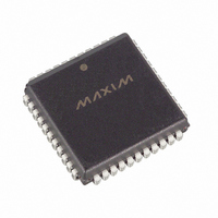
MAX547BEQH+TD Maxim Integrated Products, MAX547BEQH+TD Datasheet - Page 7

MAX547BEQH+TD
Manufacturer Part Number
MAX547BEQH+TD
Description
IC DAC 13BIT OCTAL PAR 44-PLCC
Manufacturer
Maxim Integrated Products
Datasheet
1.MAX547BCQH-D.pdf
(16 pages)
Specifications of MAX547BEQH+TD
Settling Time
5µs
Number Of Bits
13
Data Interface
Parallel
Number Of Converters
8
Voltage Supply Source
Dual ±
Power Dissipation (max)
1.07W
Operating Temperature
-40°C ~ 85°C
Mounting Type
Surface Mount
Package / Case
44-LCC, 44-PLCC
Lead Free Status / RoHS Status
Lead free / RoHS Compliant
The MAX547 contains eight 13-bit, voltage-output
DACs. These DACs are “inverted” R-2R ladder net-
works that convert 13-bit digital inputs into equivalent
analog output voltages, in proportion to the applied ref-
erence voltages. The MAX547 has one reference input
(REF_) and one analog-ground input (AGND_) for each
pair of DACs. The four REF_ inputs allow different full-
scale output voltages for each DAC pair, and the four
AGND_ inputs allow different offset voltages for each
DAC pair.
The DAC ladder outputs are buffered with op amps that
operate with a gain of two. The inverting node of the
amplifier is connected to the respective reference
input, resulting in bipolar output voltages from -REF_ to
4095/4096 REF_. Figure 1 shows the simplified DAC
circuit.
_________________________________________________Pin Description (continued)
_______________Detailed Description
PLCC
19–31
16
17
18
32
33
34
35
36
38
39
40
41
43
44
PIN
PACK
13–25
FLAT
10
11
12
26
27
28
29
30
32
33
34
35
37
38
_______________________________________________________________________________________
AGNDGH
AGNDEF
D12–D0
REFGH
VOUTH
VOUTG
VOUTF
VOUTE
NAME
REFEF
–
L
—
–
L
—
GND
D
D
A2
A1
A0
—
—
G
E
—
—
F
H
–
–
Address Bit 2
Address Bit 1
Address Bit 0
Data Bits 12–0
Load Input (active low). Driving this asynchronous input low transfers the contents of input latches
E and F to the respective DAC latches.
Load Input (active low). Driving this asynchronous input low transfers the contents of input latches
G and H to the respective DAC latches.
Digital Ground
Analog Ground for DAC G and DAC H
Reference Voltage Input for DAC G and DAC H. Bypass to AGNDGH with a 0.1µF to 1µF capacitor.
DAC H Output Voltage
DAC G Output Voltage
DAC F Output Voltage
DAC E Output Voltage
Reference Voltage Input for DAC E and DAC F. Bypass to AGNDEF with a 0.1µF to 1µF capaci-
Analog Ground for DAC E and DAC F
Analog Section
Octal, 13-Bit Voltage-Output
DAC with Parallel Interface
Figure 1. DAC Simplified Circuit Diagram
AGND –
REF –
FUNCTION
2R
2R
D0
R
2R
D10
R
2R
D11
R
R
V
2R
DAC
D12
R
OUT
7


