MAX547ACMH Maxim Integrated Products, MAX547ACMH Datasheet - Page 6
MAX547ACMH
Manufacturer Part Number
MAX547ACMH
Description
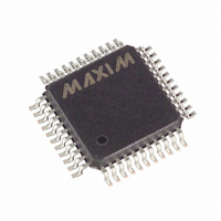
IC DAC OCTL V-OUT 13BIT 44-MQFP
Manufacturer
Maxim Integrated Products
Datasheet
1.MAX547BCQH-D.pdf
(16 pages)
Specifications of MAX547ACMH
Settling Time
5µs
Number Of Bits
13
Data Interface
Parallel
Number Of Converters
8
Voltage Supply Source
Dual ±
Power Dissipation (max)
889mW
Operating Temperature
0°C ~ 70°C
Mounting Type
Surface Mount
Package / Case
44-MQFP, 44-PQFP
Lead Free Status / RoHS Status
Contains lead / RoHS non-compliant
Available stocks
Company
Part Number
Manufacturer
Quantity
Price
Company:

Part Number:
MAX547ACMH
Manufacturer:
MAXIM
Quantity:
21
Company:
Part Number:
MAX547ACMH
Manufacturer:
MAXIM
Quantity:
5 510
Part Number:
MAX547ACMH
Manufacturer:
MAXIM/美信
Quantity:
20 000
Company:
Part Number:
MAX547ACMH+
Manufacturer:
Maxim Integrated
Quantity:
10 000
Company:
Part Number:
MAX547ACMH+T
Manufacturer:
MAXIM
Quantity:
35
Company:
Part Number:
MAX547ACMH+T
Manufacturer:
Maxim Integrated
Quantity:
10 000


Octal, 13-Bit Voltage-Output
DAC with Parallel Interface
6
(V
______________________________________________________________Pin Description
____________________________Typical Operating Characteristics (continued)
PLCC
DD
4, 42
9, 37
10
11
12
13
14
15
_______________________________________________________________________________________
1
2
3
5
6
7
8
= 5V, V
PIN
A: DIGITAL INPUTS, DAC A, DATA BITS from ALL Os to OAAAhex
B: OUTPUT, DAC B
PACK
42, 36
FLAT
3, 31
SS
40
41
43
44
ADJACENT-CHANNEL CROSSTALK
39
1
2
4
5
6
7
8
9
REF – = 4.096V, C
= -5V, REF_ = 4.096V, AGND_ = GND = 0V, T
AGNDCD
AGNDAB
REFCD
VOUTD
VOUTC
VOUTB
VOUTA
REFAB
NAME
–
L
–
L
—
—
–
C
V
V
D
–
W
—
D
–
C
500ns/div
—
—
—
—
DD
—
L
SS
C
A
S
—
—
–
R
R
–
L
–
B
D
–
–
= 50pF, R
Clear Input (active low). Driving this asynchronous input low sets the content of all latches to
1000hex. All DAC outputs are reset to AGND_.
Analog Ground for DAC C and DAC D
Reference Voltage Input for DAC C and DAC D. Bypass to AGNDCD with a 0.1µF to 1µF capacitor.
Negative Power Supply, -5V (2 pins). Connect both pins to the supply voltage. Bypass each pin
to the system analog ground with a 0.1µF to 1µF capacitor.
DAC D Output Voltage
DAC C Output Voltage
DAC B Output Voltage
DAC A Output Voltage
Positive Power Supply, 5V (2 pins). Connect both pins to the supply voltage. Bypass each pin to
the system analog ground with a 0.1µF to 1µF capacitor.
Reference Voltage Input for DAC A and DAC B. Bypass to AGNDAB with a 0.1µF to 1µF capacitor.
Analog Ground for DAC A and DAC B
Load Input (active low). Driving this asynchronous input low transfers the contents of input latches
A and B to the respective DAC latches.
Load Input (active low). Driving this asynchronous input low transfers the contents of input latches
C and D to the respective DAC latches.
Chip Select (active low)
Write Input (active low).
L
= 10k
B
5mV/div
A
5V/div
–
W
—
R
–
, along with
A
= +25°C, unless otherwise noted.)
–
C
—
S
–
, loads data into the DAC input latch selected by A0–A2.
FUNCTION
A: DIGITAL INPUTS, DAC A, DATA BITS from OAAAhex to ALL Os
B: OUTPUT, DAC B
ADJACENT-CHANNEL CROSSTALK
REF – = 4.096V, C
500ns/div
L
= 50pF, R
L
= 10k
B:
5mV/div
A:
5V/div
Related parts for MAX547ACMH
Image
Part Number
Description
Manufacturer
Datasheet
Request
R

Part Number:
Description:
Manufacturer:
Maxim Integrated Products
Datasheet:

Part Number:
Description:
Max547 Octal, 13-bit Voltage-output Dac With Parallel Interface
Manufacturer:
Maxim Integrated Products, Inc.
Datasheet:
Part Number:
Description:
MAX7528KCWPMaxim Integrated Products [CMOS Dual 8-Bit Buffered Multiplying DACs]
Manufacturer:
Maxim Integrated Products
Datasheet:
Part Number:
Description:
Single +5V, fully integrated, 1.25Gbps laser diode driver.
Manufacturer:
Maxim Integrated Products
Datasheet:
Part Number:
Description:
Single +5V, fully integrated, 155Mbps laser diode driver.
Manufacturer:
Maxim Integrated Products
Datasheet:
Part Number:
Description:
VRD11/VRD10, K8 Rev F 2/3/4-Phase PWM Controllers with Integrated Dual MOSFET Drivers
Manufacturer:
Maxim Integrated Products
Datasheet:
Part Number:
Description:
Highly Integrated Level 2 SMBus Battery Chargers
Manufacturer:
Maxim Integrated Products
Datasheet:
Part Number:
Description:
Current Monitor and Accumulator with Integrated Sense Resistor; ; Temperature Range: -40°C to +85°C
Manufacturer:
Maxim Integrated Products
Part Number:
Description:
TSSOP 14/A°/RS-485 Transceivers with Integrated 100O/120O Termination Resis
Manufacturer:
Maxim Integrated Products
Part Number:
Description:
TSSOP 14/A°/RS-485 Transceivers with Integrated 100O/120O Termination Resis
Manufacturer:
Maxim Integrated Products
Part Number:
Description:
QFN 16/A°/AC-DC and DC-DC Peak-Current-Mode Converters with Integrated Step
Manufacturer:
Maxim Integrated Products
Part Number:
Description:
TDFN/A/65V, 1A, 600KHZ, SYNCHRONOUS STEP-DOWN REGULATOR WITH INTEGRATED SWI
Manufacturer:
Maxim Integrated Products
Part Number:
Description:
Integrated Temperature Controller f
Manufacturer:
Maxim Integrated Products
Part Number:
Description:
SOT23-6/I°/45MHz to 650MHz, Integrated IF VCOs with Differential Output
Manufacturer:
Maxim Integrated Products
Part Number:
Description:
SOT23-6/I°/45MHz to 650MHz, Integrated IF VCOs with Differential Output
Manufacturer:
Maxim Integrated Products