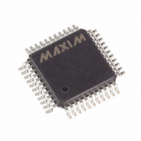
MAX547ACMH+ Maxim Integrated Products, MAX547ACMH+ Datasheet

MAX547ACMH+
Specifications of MAX547ACMH+
Related parts for MAX547ACMH+
MAX547ACMH+ Summary of contents
Page 1
... PLASTIC FP ________________________________________________________________ Maxim Integrated Products For free samples & the latest literature: http://www.maxim-ic.com, or phone 1-800-998-8800 Octal, 13-Bit Voltage-Output DAC with Parallel Interface _____________________________Features Full 13-Bit Performance without Adjustments 8 DACs in One Package Buffered Voltage Outputs Calibrated Linearity Guaranteed Monotonic to 13 Bits ± ...
Page 2
Octal, 13-Bit Voltage-Output DAC with Parallel Interface ABSOLUTE MAXIMUM RATINGS V to GND ..............................................................-0. GND...............................................................-6V to +0.3V SS Digital Input Voltage to GND ......................-0. REF_ ..........................................(AGND_ - 0.3V AGND_ .............................................(V SS ...
Page 3
ELECTRICAL CHARACTERISTICS (continued +5V -5V, REF_ = 4.096V, AGND_ = GND = 0V Typical values are +25°C.) A PARAMETER SYMBOL POWER SUPPLIES Positive Supply Range V DD Negative Supply Range ...
Page 4
Octal, 13-Bit Voltage-Output DAC with Parallel Interface __________________________________________Typical Operating Characteristics ( -5V, REF_ = 4.096V, AGND_ = GND = 0V RELATIVE ACCURACY vs. DIGITAL INPUT CODE 0.5 0.4 0.3 0.2 0.1 0 -0.1 ...
Page 5
Operating Characteristics (continued 5V -5V, REF_ = 4.096V, AGND_ = GND = 0V POWER-SUPPLY REJECTION RATIO vs. FREQUENCY 0 - ±200mV LOAD -20 -30 ...
Page 6
Octal, 13-Bit Voltage-Output DAC with Parallel Interface ____________________________Typical Operating Characteristics (continued 5V -5V, REF_ = 4.096V, AGND_ = GND = 0V ADJACENT-CHANNEL CROSSTALK 500ns/div REF – = 4.096V 50pF ...
Page 7
Description (continued) PIN NAME FLAT PLCC PACK Address Bit Address Bit Address Bit 0 19–31 13–25 D12–D0 Data Bits 12–0 – — — — – Load Input (active ...
Page 8
Octal, 13-Bit Voltage-Output DAC with Parallel Interface Reference and Analog-Ground Inputs The REF_ inputs can range between AGND_ and V However, the DAC outputs will operate to V and V + 0.6V, due to the output amplifiers’ voltage- SS swing ...
Page 9
Table 2. Interface Truth Table – — — – – — — – – — – – — – – Both latches transparent ...
Page 10
Octal, 13-Bit Voltage-Output DAC with Parallel Interface Table 3. MAX547 Bipolar Code Table (AGND_ = 0V) INPUT 1 1111 1111 1111 +REF_ 1 0000 0000 0001 +REF_ 1 0000 0000 0000 0 1111 1111 1111 -REF_ 0 0000 0000 0001 ...
Page 11
Table 5. Reference, AGND – and Output Relationships BIPOLAR OPERATION PARAMETER Bipolar Zero Level, or Unipolar Mid-scale, (Code = 1000000000000) Differential Reference Voltage ( Negative Full-scale Output (Code = All 0s) Positive Full-Scale Output (Code = All 1s) ...
Page 12
Octal, 13-Bit Voltage-Output DAC with Parallel Interface + - MAX494 Figure 6. Reference Buffering Power-Supply Bypassing and Ground Management For optimum performance, use a multilayer PC board with an unbroken analog ground. For normal opera- tion, when all AGND_ pins ...
Page 13
Diagram INPUT LATCH A INPUT LATCH B INPUT LATCH C INPUT LATCH D D12–D0 DATA BUS INPUT LATCH E INPUT LATCH F INPUT LATCH G INPUT LATCH 16, 18 A0–A2 ...
Page 14
Octal, 13-Bit Voltage-Output DAC with Parallel Interface ____________________________________________________________Chip Topography VOUTB VOUTA V DD REFAB AGNDAB LDAB LDCD TRANSISTOR COUNT: 8987 SUBSTRATE CONNECTED ______________________________________________________________________________________ VOUTG VOUTH V DD REFGH AGNDGH GND LDGH LDEF ...
Page 15
Information ______________________________________________________________________________________ Octal, 13-Bit Voltage-Output DAC with Parallel Interface INCHES MILLIMETERS DIM MIN MAX MIN MAX A 0.165 0.180 4.19 4.57 A1 0.100 0.110 2.54 ...
Page 16
... Maxim cannot assume responsibility for use of any circuitry other than circuitry entirely embodied in a Maxim product. No circuit patent licenses are implied. Maxim reserves the right to change the circuitry and specifications without notice at any time. 16 __________________Maxim Integrated Products, 120 San Gabriel Drive, Sunnyvale, CA 94086 (408) 737-7600 © 1995 Maxim Integrated Products Printed USA is a registered trademark of Maxim Integrated Products ...


