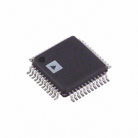
AD1953YST Analog Devices Inc, AD1953YST Datasheet - Page 7

AD1953YST
Manufacturer Part Number
AD1953YST
Description
IC DAC AUDIO 3CH 26BIT 48-LQFP
Manufacturer
Analog Devices Inc
Series
SigmaDSP®r
Datasheet
1.AD1953YSTZRL.pdf
(36 pages)
Specifications of AD1953YST
Rohs Status
RoHS non-compliant
Number Of Bits
26
Data Interface
Serial
Number Of Converters
3
Voltage Supply Source
Analog and Digital
Power Dissipation (max)
540mW
Operating Temperature
-40°C ~ 105°C
Mounting Type
Surface Mount
Package / Case
48-LQFP
For Use With
EVAL-AD1953EBZ - BOARD EVAL FOR AD1953 3CH 24BIT
Settling Time
-
Available stocks
Company
Part Number
Manufacturer
Quantity
Price
Company:
Part Number:
AD1953YSTZ
Manufacturer:
AD
Quantity:
1 450
Company:
Part Number:
AD1953YSTZ
Manufacturer:
ADI
Quantity:
455
Company:
Part Number:
AD1953YSTZ
Manufacturer:
Analog Devices Inc
Quantity:
10 000
Company:
Part Number:
AD1953YSTZRL
Manufacturer:
Analog Devices Inc
Quantity:
10 000
Company:
Part Number:
AD1953YSTZRL7
Manufacturer:
Analog Devices Inc
Quantity:
10 000
10
11
12
13
14
15
16
17
18
19
20
21
22
23
24
25
26
27
28
29
30
31
32
33
34
35
36
37
38
39
40
41
42
43
44
45
46
47
48
REV. 0
1
2
3
4
5
6
7
8
9
Pin No.
Mnemonic
NC
MCLK2
MCLK1
MCLK0
AUXDATA
MUTE
DVDD
SDATA2
BCLK2
LRCLK2
SDATA1
BCLK1
DGND
LRCLK1
SDATA0
BCLK0
LRCLK0
CDATA
CCLK
CLATCH
RESETB
AVDD
AGND
NC
VOUTS–
VOUTS+
AGND
VOUTR–
VOUTR+
AVDD
AGND
AVDD
VOUTL+
VOUTL–
AGND
NC
NC
VREF
FILTCAP
ZEROFLAG
DMUXO/TDMO
BMUXO/TDMBC
LRMUXO/TDMFS
ODVDD
DCSOUT
COUT
MCLKOUT
DGND
Input/
Output
IN
IN
IN
IN
IN
IN
IN
IN
IN
IN
IN
IN
IN
IN
IN
IN
IN
IN
OUT
OUT
OUT
OUT
OUT
OUT
IN
IN
OUT
OUT
OUT
OUT
OUT
OUT
OUT
PIN FUNCTION DESCRIPTIONS
Description
No Connect
Master Clock Input 2 256/512 f
Master Clock Input 1 256/512 f
Master Clock Input 0 256/512 f
Auxiliary Serial Data Input
Mute Signal, Initiates Volume Ramp-Down
Digital Supply for DSP Core, 4.5 V to 5.5 V
Serial Data Input 2
Bit Clock 2
Left/Right Clock 2
Serial Data Input 1
Bit Clock 1
Digital Ground
Left/Right Clock 1
Serial Data Input 0
Bit Clock 0
Left/Right Clock 0
SPI Data Input
SPI Data Bit Clock
SPI Data Framing Signal
Reset Signal, Active Low
Analog 5 V Supply
Analog GND
No Connect
Negative Sub Analog DAC Output
Positive Sub Analog DAC Output
Analog GND
Negative Left Analog DAC Output
Positive Left Analog DAC Output
Analog 5 V Supply
Analog GND
Analog 5 V Supply
Positive Left Analog DAC Output
Negative Left Analog DAC Output
Analog GND
No Connect
No Connect
Connection for Filtered AVDD/2
Connection for Noise Reduction Capacitor
Zero Flag Output. High when both left and right channels are 0 for 1024 frames.
Dual-function Pin: Serial Data MUX Output/TDM Mode Output Data
Dual-function Pin: Bit Clock MUX Output/TDM Mode Bit Clock Output (256 f
Dual-function Pin: Left/Right Clock MUX Output/TDM Mode Frame Sync
Clock Output
Digital Supply Pin for Output Drivers, 2.5 V to 5.5 V
Data Capture Serial Output for Data Capture Registers. Use in conjunction
with selected LRCLK and BCLK to form a 3-wire output.
SPI Data Output, Three-Stated when Inactive
Master Clock Output 512/256 f
Digital Ground
–7–
S
S
S
S
(Frequency Selected by SPI Register)
AD1953
S
)


