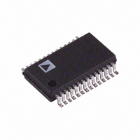
AD1854JRS Analog Devices Inc, AD1854JRS Datasheet - Page 7

AD1854JRS
Manufacturer Part Number
AD1854JRS
Description
IC DAC STEREO 96KHZ 5V 28SSOP
Manufacturer
Analog Devices Inc
Datasheet
1.AD1854JRSZ.pdf
(12 pages)
Specifications of AD1854JRS
Rohs Status
RoHS non-compliant
Number Of Bits
20
Data Interface
DSP, I²S, Serial
Number Of Converters
2
Voltage Supply Source
Analog and Digital
Power Dissipation (max)
250mW
Operating Temperature
0°C ~ 70°C
Mounting Type
Surface Mount
Package / Case
28-SSOP
For Use With
EVAL-AD1854EB - BOARD EVAL FOR AD1854
Settling Time
-
Available stocks
Company
Part Number
Manufacturer
Quantity
Price
Company:
Part Number:
AD1854JRS
Manufacturer:
MOTOROLA
Quantity:
1 157
Part Number:
AD1854JRS
Manufacturer:
ADI/亚德诺
Quantity:
20 000
Company:
Part Number:
AD1854JRSZ
Manufacturer:
ADI
Quantity:
26
Part Number:
AD1854JRSZ
Manufacturer:
ADI/亚德诺
Quantity:
20 000
Serial Control Port
The AD1854 serial control port is SPI-compatible. SPI (Serial
Peripheral Interface) is an industry standard serial port protocol.
The write-only serial control port gives the user access to: select
input mode, soft power-down control, soft de-emphasis, channel-
specific attenuation and mute (both channels at once). The
AD1854 serial control port consists of three signals, control
clock CCLK (Pin 4), control data CDATA (Pin 5), and control
latch CLATCH (Pin 3). The control data input must be valid
on the control clock rising edge, and the control clock must make a
LO to HI transition when there is valid data. The control latch
must make a LO-to-HI transition after the LSB has been clocked
into the AD1854, while the control clock is inactive. The timing
relation between these signals is shown in Figure 5. The control
bits are assigned as in Table IV.
t
t
t
t
t
t
t
REV. A
Data 15 Data 14 Data 13 Data 12
MSB
IDPM1 IDPM0
Input
Mode1
Select
CCH
CCL
CCP
CSU
CHD
CLL
CLH
L/RCLK
SDATA
L/RCLK
SDATA
INPUT
INPUT
INPUT
INPUT
INPUT
BCLK
INPUT
BCLK
CCLK HI Pulsewidth
CCLK LO Pulsewidth
CCLK Period
CDATA Setup Time
CDATA Hold Time
CLATCH LO Pulsewidth
CLATCH HI Pulsewidth
Input
Mode0
Select
LSB
Soft
Power- De-
Down
CLATCH
CDATA
MSB
Table III. Digital Timing
CCLK
MSB
MSB–1
Soft
Emphasis (Nonmute)
MSB–2
MSB–1
LEFT CHANNEL
t
t
CCL
CCP
D15
MSB–2
Data 11
1/Mute
0/Normal
t
CCH
LEFT CHANNEL
Min
40 (Burst Mode)
40 (Burst Mode)
80 (Burst Mode)
10
10
10
130 (Burst Mode)
LSB+2
t
D14
CSU
t
LSB+1
CHD
Data 10 Data 9
1/Right
0/Left
Table IV. Serial Control Bit Definitions
Figure 5. Serial Control Port Timing
LSB
Figure 4. 32 × F
LSB+2
Figure 3. Left-Justified Mode
Volume Volume Volume
Control Control Control
Data
LSB+1
Unit
ns
ns
ns
ns
ns
ns
ns
Data 8
Data
LSB
–7–
S
Data 7
Data
MSB
MSB
Packed Mode
The serial control port is byte oriented. The data is MSB first,
and is unsigned. There is one control register for the left
channel or the right channel, as distinguished by Bit Data 10.
For power-up and reset, the default settings are: Data 11 the
mute control bit, reset default state is LO, which is the normal
(nonmuted) setting. Data 10 is LO, the Volume 9 through
Volume 0 control bits have a reset default value of 11 1111 1111,
which is an attenuation of 0.0 dB (i.e., full scale, no attenuation).
The intent with these reset defaults is to enable AD1854 applica-
tions without requiring the use of the serial control port. For those
users who do not use the serial control port, it is still possible to
mute the AD1854 output by using the MUTE (Pin 23) signal.
Note that the serial control port timing is asynchronous to the
serial data port timing. Changes made to the attenuator level
will be updated on the next edge of the L/RCLK after the
CLATCH write pulse as shown in Figure 8.
The SPI port can be used in either of two modes, Burst Mode,
or Continuous CCLK Mode, as described below.
Continuous CCLK Mode
In this mode, the maximum CCLK frequency is 3 MHz. The
CCLK can run continuously between transactions. Please note
that the LO-to-HI transition of the CLATCH with respect to
the rising edge of CCLK must be at least 130 ns, as shown in
Figure 6.
RIGHT CHANNEL
MSB–1
MSB–1
Data 6
Volume
Control
Data
MSB–2
MSB–2
Data 5
Volume
Control
Data
RIGHT CHANNEL
LSB+2
Data 4
Volume
Control
Data
LSB+1
D0
LSB+2
LSB
t
CLL
Data 3
Volume
Control
Data
LSB+1
t
CLH
LSB
Data 2
Volume
Control
Data
MSB
AD1854
Volume Volume
Data 1
Control Control
Data
MSB
MSB–1
MSB–1
LSB
Data 0
Data


