AD8600AP Analog Devices Inc, AD8600AP Datasheet
AD8600AP
Specifications of AD8600AP
Available stocks


Related parts for AD8600AP


AD8600AP Summary of contents
Page 1
FEATURES 16 Independently Addressable Voltage Outputs Full-Scale Set by External Reference 2 s Settling Time Double Buffered 8-Bit Parallel Input High Speed Data Load Rate Data Readback Operates from Single +5 V Optional 6 V Supply Extends Output Range ...
Page 2
AD8600–SPECIFICATIONS SINGLE SUPPLY (@ DD1 DD2 Parameter Symbol 1 STATIC PERFORMANCE Resolution N 2 Relative Accuracy INL 2 Differential Nonlinearity DNL Full-Scale Voltage V FS Full-Scale Tempco TCV FS Zero Scale Error V ZSE V ...
Page 3
DUAL SUPPLY (@ DD1 DD2 CC Parameter Symbol 1 STATIC PERFORMANCE Resolution N Total Unadjusted Error TUE Relative Accuracy INL Differential Nonlinearity DNL Full-Scale Voltage V FS Full-Scale Voltage Error V FSE Full-Scale Tempco TCV ...
Page 4
AD8600 ELECTRICAL CHARACTERISTICS Parameter 1, 2 INTERFACE TIMING Clock (EN) Frequency Clock (EN) High Pulse Width Clock (EN) LowPulse Width Data Setup Time Data Hold Time Address Setup Time Address Hold Time Valid Address to Data Valid Load Enable Setup ...
Page 5
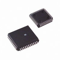
... CONNECT ORDERING GUIDE Package Model Temperature Description AD8600AP – +85 C 44-Lead PLCC AD8600Chips +25 C Die* *For die specifications contact your local Analog Devices sales office. The AD8600 contains 5782 transistors. CAUTION ESD (electrostatic discharge) sensitive device. Electrostatic charges as high as 4000 V readily accumulate on the human body and test equipment and can discharge without detection ...
Page 6
AD8600 TRANSFER EQUATIONS Output Voltage V REF 256 where i is the DAC channel number and D is the decimal value of the DAC register data. Table I. Truth Table EN R Operation ...
Page 7
DACs 00–07 SUPERIMPOSED +5V –1 – +3.5V REF +1/2 0 DACs 08–015 SUPERIMPOSED –1 128 192 256 DIGITAL INPUT CODE – Decimal Figure ...
Page 8
AD8600 + – 3.5V REF –75 –50 – TEMPERATURE – C Figure 14. Supply Current vs. Temperature Operation The AD8600 is a 16-channel ...
Page 9
Power Supply and Grounding Considerations The low power consumption of the AD8600 is a direct result of circuit design optimizing using a CBCMOS process. The over- all power dissipation of 120 mW translates to a total supply cur- rent of ...
Page 10
AD8600 Interface Timing and Control The AD8600 employs a double buffered DAC structure with each DAC channel having a unique input register and DAC reg- ister as shown in the diagram entitled “Equivalent DAC Chan- nel” on the first page ...
Page 11
Unipolar Output Operation The AD8600 is configured to give unipolar operation. The full- scale output voltage is equivalent to the reference input voltage minus 1 LSB. The output is dependent upon the digital code and follows Table III. The actual ...
Page 12
AD8600 * This program contains subroutines to read and write * to the AD8600 from the 68HC11. * program has been included, to continuously ramp the * output giving a triangle wave output The following connections need to ...
Page 13
DAC address ldaa 0,x load the address from 68HC11 mem staa portb set the address on portb * LD, CS, EN, R/W are all low for * transparent DAC ...
Page 14
AD8600 The functionality of this circuit is shown in the scope photo in Figure 24 The top trace is the control ramp, which goes from 1.25 V. The bottom trace is the output of the AD600. The ...
Page 15
Plastic Lead Chip Carrier (PLCC) Package 0.048 (1.21) 0.042 (1.07) 0.020 (0.50) R REV. 0 OUTLINE DIMENSIONS Dimensions shown in inches and (mm). (P-44A) 0.180 (4.57) 0.165 (4.19) 0.048 (1.21) 0.056 (1.42) 0.042 (1.07) 0.042 (1.07 ...
Page 16
AD8600 –16– REV. 0 ...