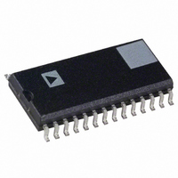
AD9731BR Analog Devices Inc, AD9731BR Datasheet - Page 5

AD9731BR
Manufacturer Part Number
AD9731BR
Description
IC DAC 10BIT 170MSPS 28-SOIC
Manufacturer
Analog Devices Inc
Datasheet
1.AD9731BR.pdf
(12 pages)
Specifications of AD9731BR
Rohs Status
RoHS non-compliant
Settling Time
3.8ns
Number Of Bits
10
Data Interface
Parallel
Number Of Converters
1
Voltage Supply Source
Analog and Digital, Dual ±
Power Dissipation (max)
449mW
Operating Temperature
-40°C ~ 85°C
Mounting Type
Surface Mount
Package / Case
28-SOIC (7.5mm Width)
Available stocks
Company
Part Number
Manufacturer
Quantity
Price
Part Number:
AD9731BR
Manufacturer:
ADI/亚德诺
Quantity:
20 000
Part Number:
AD9731BRSZ
Manufacturer:
ADI/亚德诺
Quantity:
20 000
Part Number:
AD9731BRZ
Manufacturer:
ADI/亚德诺
Quantity:
20 000
REV. B
Pin No.
1
2–9
10
11
12, 13
14
15, 18, 28
16
17
19
20
21
22
23
24
25
26
27
Mnemonic
D9(MSB)
D8–D1
D0(LSB)
CLOCK
NC
DIGITAL +V
GND
DIGITAL –V
R
ANALOG RETURN
I
I
ANALOG –V
REF IN
CONTROL AMP OUT
REF OUT
CONTROL AMP IN
DIGITAL –V
OUT
OUTB
SET
S
S
S
S
Function
Most significant data bit of digital input word
Eight bits of 10-bit digital input word
Least significant data bit of digital input word
TTL-compatible edge-triggered latch enable signal for on-board registers
No internal connection to this pin
5 V supply voltage for digital circuitry
Converter ground
–5.2 V supply voltage for digital circuitry
Connection for external reference set resistor; nominal 1.96 kW. Full-scale output
current = 32 (control amp in V/R
Analog return. This point and the reference side of the DAC load resistors should be
connected to the same potential (nominally ground).
Analog current output; full-scale current occurs with a digital word input of all “1s.” With
external load resistor, output voltage = I
nominally 240 W.
Complementary analog current output; full-scale current occurs with a digital word input
of all “0s.”
Negative analog supply, nominally –5.2 V
Normally connected to CONTROL AMP OUT (Pin 24). Direct line to DAC current
source network. Voltage changes (noise) at this point have a direct effect on the full-scale
output current of the DAC. Full-scale current output = 32 (CONTROL AMP IN/R
when using the internal amplifier. DAC load is virtual ground.
Normally connected to REF IN (Pin 23). Output of internal control amplifier that provides
a reference for the current switch network.
Normally connected to CONTROL AMP IN (Pin 26). Internal voltage reference,
nominally –1.25 V.
Normally connected to REF Out (Pin 25) if not connected to external reference.
Negative digital supply, nominally –5.2 V.
PIN FUNCTION DESCRIPTIONS
DIGITAL +V
D9(MSB)
D0(LSB)
CLOCK
PIN CONFIGURATION
NC
NC
D8
D7
D6
D5
D4
D3
D2
D1
S
10
11
12
13
14
NC = NO CONNECT
1
2
3
4
5
6
7
8
9
(Not to Scale)
TOP VIEW
AD9731
–5–
28
27
26
25
24
23
22
21
20
19
18
17
16
15
GND
DIGITAL –V
CONTROL AMP IN
REF OUT
CONTROL AMP OUT
REF IN
ANALOG –V
I
I
ANALOG RETURN
GND
R
DIGITAL –V
GND
SET
OUTB
OUT
SET
).
OUT
S
S
S
(R
LOAD
R
INTERNAL
). R
INTERNAL
AD9731
is
SET
)


