ATF750C-15GM/883 Atmel, ATF750C-15GM/883 Datasheet - Page 12
ATF750C-15GM/883
Manufacturer Part Number
ATF750C-15GM/883
Description
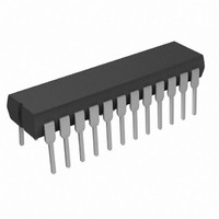
IC PLD EE CMOS 15NS 24CDIP
Manufacturer
Atmel
Series
ATF750C(L)r
Datasheet
1.ATF750C-7JC.pdf
(25 pages)
Specifications of ATF750C-15GM/883
Programmable Type
In System Programmable (min 1K program/erase cycles)
Delay Time Tpd(1) Max
15.0ns
Voltage Supply - Internal
4.5 V ~ 5.5 V
Number Of Macrocells
10
Number Of I /o
10
Operating Temperature
-55°C ~ 125°C
Mounting Type
Through Hole
Package / Case
24-CDIP (0.300", 7.62mm)
Features
Programmable
Voltage
5V
Memory Type
CMOS
Lead Free Status / RoHS Status
Lead free / RoHS Compliant
Number Of Logic Elements/cells
-
Available stocks
Company
Part Number
Manufacturer
Quantity
Price
Company:

Part Number:
ATF750C-15GM/883
Manufacturer:
ATMEL
Quantity:
32


23. Using the ATF750C’s Many Advanced Features
24. Synchronous Preset and Asynchronous Reset
25. Software Support
12
ATF750C(L)
The ATF750C(L)’s advanced flexibility packs more usable gates into 24 pins than any other logic
device. The ATF750C(L)s start with the popular 22V10 architecture, and add several enhanced
features:
One synchronous preset line is provided for all 20 registers in the ATF750C(L). The appropriate
input signals to cause the internal clocks to go to a high state must be received during a syn-
chronous preset. Appropriate setup and hold times must be met, as shown in the switching
waveform diagram.
An individual asynchronous reset line is provided for each of the 20 flip-flops. Both master and
slave halves of the flip-flops are reset when the input signals received force the internal resets
high.
All family members of the ATF750C(L) can be designed with Atmel
Additionally, the ATF750C may be programmed to perform the ATV750(L) functional subset (no
T-type flip-flops, pin clocking or D/T2 feedback) using the ATV750 JEDEC file. In this case, the
ATF750C becomes a direct replacement or speed upgrade for the ATV750. The ATF750C is a
direct replacement for the ATV750(L) and the ATV750B(L).
• Selectable D- and T-type Registers
• Selectable Asynchronous Clocks
• A Full Bank of Ten More Registers
• Independent I/O Pin and Feedback Paths
Each ATF750C(L) flip-flop can be individually configured as either D- or T-type. Using the T-
type configuration, JK and SR flip-flops are also easily created. These options allow more
efficient product term usage.
Each of the ATF750C(L)’s flip-flops may be clocked by its own clock product term or directly
from Pin 1 (SMD Lead 2). This removes the constraint that all registers must use the same
clock. Buried state machines, counters and registers can all coexist in one device while
running on separate clocks. Individual flip-flop clock source selection further allows mixing
higher performance pin clocking and flexible product term clocking within one design.
The ATF750C(L) provides two flip-flops per output logic cell for a total of 20. Each register
has its own sum term, its own reset term and its own clock term.
Each I/O pin on the ATF750C(L) has a dedicated input path. Each of the 20 registers has its
own feedback terms into the array as well. This feature, combined with individual product
terms for each I/O’s output enable, facilitates true bi-directional I/O design.
®
-WinCUPL.
0776L–PLD–11/08
Related parts for ATF750C-15GM/883
Image
Part Number
Description
Manufacturer
Datasheet
Request
R

Part Number:
Description:
IC PLD HS 750 GATE 5.0V 24-SOIC
Manufacturer:
Atmel
Datasheet:

Part Number:
Description:
IC PLD HS 750 GATE 5.0V 24-PDIP
Manufacturer:
Atmel
Datasheet:

Part Number:
Description:
IC CPLD 10NS 28PLCC
Manufacturer:
Atmel
Datasheet:
Part Number:
Description:
IC CPLD 20 MACROCELL 15NS 28PLCC
Manufacturer:
Atmel
Datasheet:
Part Number:
Description:
IC CPLD 10NS 24SOIC
Manufacturer:
Atmel
Datasheet:
Part Number:
Description:
IC PLD HS 750 GATE 5.0V 24-SOIC
Manufacturer:
Atmel
Datasheet:
Part Number:
Description:
IC CPLD 7NS 24SOIC
Manufacturer:
Atmel
Datasheet:
Part Number:
Description:
IC CPLD 15NS LOW PWR 24-SOIC
Manufacturer:
Atmel
Datasheet:
Part Number:
Description:
IC CPLD 10NS 28PLCC
Manufacturer:
Atmel
Datasheet:
Part Number:
Description:
IC CPLD 10NS 28PLCC
Manufacturer:
Atmel
Datasheet:
Part Number:
Description:
IC CPLD 15NS 28PLCC
Manufacturer:
Atmel
Datasheet:
Part Number:
Description:
IC CPLD 15NS LOW PWR 24-SOIC
Manufacturer:
Atmel
Datasheet:
Part Number:
Description:
IC CPLD 7NS 28PLCC
Manufacturer:
Atmel
Datasheet:
Part Number:
Description:
IC CPLD 7NS 24SOIC
Manufacturer:
Atmel
Datasheet:
Part Number:
Description:
IC CPLD 10NS 24PDIP
Manufacturer:
Atmel
Datasheet: