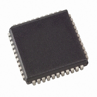
ATF1500A-10JI Atmel, ATF1500A-10JI Datasheet - Page 5

ATF1500A-10JI
Manufacturer Part Number
ATF1500A-10JI
Description
IC CPLD 10NS 44PLCC
Manufacturer
Atmel
Series
ATF1500A(L)r
Datasheet
1.ATF1500A-10JU.pdf
(19 pages)
Specifications of ATF1500A-10JI
Programmable Type
In System Programmable (min 100 program/erase cycles)
Delay Time Tpd(1) Max
10.0ns
Voltage Supply - Internal
4.5 V ~ 5.5 V
Number Of Macrocells
32
Number Of I /o
32
Operating Temperature
-40°C ~ 85°C
Mounting Type
Surface Mount
Package / Case
44-PLCC
Voltage
4.5 ~ 5.5V
Memory Type
FLASH
Lead Free Status / RoHS Status
Contains lead / RoHS non-compliant
Features
-
Number Of Logic Elements/cells
-
Other names
ATF1500A10JI
Available stocks
Company
Part Number
Manufacturer
Quantity
Price
Company:
Part Number:
ATF1500A-10JI
Manufacturer:
ATM
Quantity:
6 100
Part Number:
ATF1500A-10JI
Manufacturer:
ATMEL/爱特梅尔
Quantity:
20 000
In addition to D, T, JK and SR operation, the flip-flop can
also be configured as a flow-through latch. In this mode,
data passes through when the clock is high and is latched
when the clock is low.
The clock itself can be either the global CLK pin or an indi-
vidual product term. The flip-flop changes state on the
clock’s rising edge. When the CLK pin is used as the clock,
one of the macrocell product terms can be selected as a
clock enable. When the clock enable function is active and
the enable signal (product term) is low, all clock edges are
ignored.
The flip-flop’s asynchronous reset signal (AR) can be either
the pin global clear (GCLR), a product term, or always off.
AR can also be a logic OR of GCLR with a product term.
The asynchronous preset (AP) can be a product term or
always off.
Output Select and Enable
The ATF1500A macrocell output can be selected as regis-
tered or combinatorial. When the output is registered, the
same registered signal is fed back internally to the global
bus. When the output is combinatorial, the buried feedback
can be either the same combinatorial signal or it can be the
register output if the separate product term is chosen as
the flip-flop input.
The output enable multiplexer (MOE) controls the output
enable signals. Any buffer can be permanently enabled for
simple output operation. Buffers can also be permanently
disabled to allow use of the pin as an input. In this configu-
ration all the macrocell resources are still available, includ-
ing the buried feedback, expander and CASCADE logic.
The output enable for each macrocell can also be selected
as either of the two OE pins or as an individual product
term.
Global/Regional Busses
The global bus contains all Input and I/O pin signals as well
as the buried feedback signal from all 32 macrocells.
Together with the complement of each signal, this provides
a 68-bit bus as input to every product term. Having the
entire global bus available to each macrocell eliminates
any potential routing problems. With this architecture
designs can be modified without requiring pinout changes.
Each macrocell also generates a foldback product term.
This signal goes to the regional bus, and is available to 16
macrocells. The foldback is an inverse polarity of one of the
macrocell’s product terms. The 16 foldback terms in each
region allow generation of high fan-in sum terms (up to 21
product terms) with little additional delay.
5


