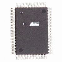
ATF1508ASL-25QI100 Atmel, ATF1508ASL-25QI100 Datasheet - Page 5

ATF1508ASL-25QI100
Manufacturer Part Number
ATF1508ASL-25QI100
Description
IC CPLD 25NS LOW PWR 100PQFP
Manufacturer
Atmel
Series
ATF1508AS(L)r
Datasheet
1.ATF1508ASL-20JC84.pdf
(31 pages)
Specifications of ATF1508ASL-25QI100
Programmable Type
In System Programmable (min 10K program/erase cycles)
Delay Time Tpd(1) Max
25.0ns
Voltage Supply - Internal
4.5 V ~ 5.5 V
Number Of Macrocells
128
Number Of I /o
80
Operating Temperature
-40°C ~ 85°C
Mounting Type
Surface Mount
Package / Case
100-MQFP, 100-PQFP
Voltage
5V
Memory Type
EEPROM
Lead Free Status / RoHS Status
Contains lead / RoHS non-compliant
Features
-
Number Of Logic Elements/cells
-
Other names
ATF1508ASL25QI100
Available stocks
Company
Part Number
Manufacturer
Quantity
Price
Flip-flop
Extra Feedback
I/O Control
Global Bus/Switch
Matrix
Foldback Bus
3.3V or 5.0V I/O
Operation
Open-collector
Output Option
0784P–PLD–7/05
The ATF1508AS’s flip-flop has very flexible data and control functions. The data input can
come from either the XOR gate, from a separate product term or directly from the I/O pin.
Selecting the separate product term allows creation of a buried registered feedback within a
combinatorial output macrocell. (This feature is automatically implemented by the fitter soft-
ware). In addition to D, T, JK and SR operation, the flip-flop can also be configured as a flow-
through latch. In this mode, data passes through when the clock is high and is latched when
the clock is low.
The clock itself can be either the Global CLK Signal (GCK) or an individual product term. The
flip-flop changes state on the clock’s rising edge. When the GCK signal is used as the clock,
one of the macrocell product terms can be selected as a clock enable. When the clock enable
function is active and the enable signal (product term) is low, all clock edges are ignored. The
flip-flop’s asynchronous reset signal (AR) can be either the Global Clear (GCLEAR), a product
term, or always off. AR can also be a logic OR of GCLEAR with a product term. The asynchro-
nous preset (AP) can be a product term or always off.
The ATF15xxSE Family macrocell output can be selected as registered or combinatorial. The
extra buried feedback signal can be either combinatorial or a registered signal regardless of
whether the output is combinatorial or registered. (This enhancement function is automatically
implemented by the fitter software.) Feedback of a buried combinatorial output allows the cre-
ation of a second latch within a macrocell.
The output enable multiplexer (MOE) controls the output enable signal. Each I/O can be indi-
vidually configured as an input, output or for bi-directional operation. The output enable for
each macrocell can be selected from the true or compliment of the two output enable pins, a
subset of the I/O pins, or a subset of the I/O macrocells. This selection is automatically done
by the fitter software when the I/O is configured as an input, all macrocell resources are still
available, including the buried feedback, expander and cascade logic.
The global bus contains all input and I/O pin signals as well as the buried feedback signal from
all 128 macrocells. The switch matrix in each logic block receives as its inputs all signals from
the global bus. Under software control, up to 40 of these signals can be selected as inputs to
the logic block.
Each macrocell also generates a foldback product term. This signal goes to the regional bus
and is available to 16 macrocells. The foldback is an inverse polarity of one of the macrocell’s
product terms. The 16 foldback terms in each region allows generation of high fan-in sum
terms (up to 21 product terms) with a little additional delay.
The ATF1508AS device has two sets of V
always be connected to a 5.0V power supply. V
patible” with both 3.3V and 5.0V inputs. V
connected for 3.3/5.0V power supply.
This option enables the device output to provide control signals such as an interrupt that can
be asserted by any of the several devices.
CC
CCIO
pins viz, V
CCINT
pins are for I/O output drives and can be
pins are for input buffers and are “com-
CCINT
and V
ATF1508AS(L)
CCIO
. V
CCINT
pins must
5


