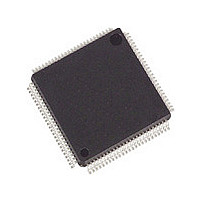
ADSP-2185NBST-320 Analog Devices Inc, ADSP-2185NBST-320 Datasheet - Page 26

ADSP-2185NBST-320
Manufacturer Part Number
ADSP-2185NBST-320
Description
IC DSP CONTROLLER 16BIT 100LQFP
Manufacturer
Analog Devices Inc
Series
ADSP-21xxr
Type
Fixed Pointr
Datasheet
1.ADSP-2185NKSTZ-320.pdf
(48 pages)
Specifications of ADSP-2185NBST-320
Rohs Status
RoHS non-compliant
Interface
Host Interface, Serial Port
Clock Rate
80MHz
Non-volatile Memory
External
On-chip Ram
80kB
Voltage - I/o
1.8V, 2.5V, 3.3V
Voltage - Core
1.90V
Operating Temperature
-40°C ~ 85°C
Mounting Type
Surface Mount
Package / Case
100-LQFP
Device Core Size
16b
Architecture
Enhanced Harvard
Format
Fixed Point
Clock Freq (max)
80MHz
Mips
80
Device Input Clock Speed
80MHz
Ram Size
80KB
Program Memory Size
Not RequiredKB
Operating Supply Voltage (typ)
2.5/3.3V
Operating Supply Voltage (min)
1.8V
Operating Supply Voltage (max)
2/3.6V
Operating Temp Range
-40C to 85C
Operating Temperature Classification
Industrial
Mounting
Surface Mount
Pin Count
100
Package Type
LQFP
Lead Free Status / Rohs Status
Not Compliant
Available stocks
Company
Part Number
Manufacturer
Quantity
Price
Company:
Part Number:
ADSP-2185NBST-320
Manufacturer:
AD
Quantity:
1 831
ADSP-218xN
TIMING SPECIFICATIONS
This section contains timing information for the DSP’s
external signals.
General Notes
Use the exact timing information given. Do not attempt to
derive parameters from the addition or subtraction of others.
While addition or subtraction would yield meaningful results
for an individual device, the values given in this data sheet
reflect statistical variations and worst cases. Consequently,
parameters cannot be added up meaningfully to derive
longer times.
Timing Notes
Switching characteristics specify how the processor changes its
signals. Designers have no control over this timing—circuitry
external to the processor must be designed for compatibility
with these signal characteristics. Switching characteristics tell
what the processor will do in a given circumstance. Switching
characteristics can also be used to ensure that any timing
requirement of a device connected to the processor (such as
memory) is satisfied.
Timing requirements apply to signals that are controlled by cir-
cuitry external to the processor, such as the data input for a read
operation. Timing requirements guarantee that the processor
operates correctly with other devices.
Frequency Dependency For Timing Specifications
t
with a frequency equal to half the instruction rate. For example,
a 40 MHz input clock (which is equivalent to 25 ns) yields a
12.5 ns processor cycle (equivalent to 80 MHz). t
within the range of 0.5 t
relevant timing parameters to obtain the specification value.
Example: t
Output Drive Currents
Figure 21
ers on the ADSP-218xN series.The curves represent the current
drive capability of the output drivers as a function of
output voltage.
Figure 23
Capacitive Loading
Figure 24
tics of the ADSP-218xN.
CK
is defined as 0.5 t
shows typical I-V characteristics for the output driv-
shows the typical power-down supply current.
and
CKH
Figure 25
= 0.5 t
CKI
CK
. The ADSP-218xN uses an input clock
– 2 ns = 0.5 (12.5 ns) – 2 ns = 4.25 ns
CKI
show the capacitive loading characteris-
period should be substituted for all
CK
Rev. A | Page 26 of 48 | August 2006
values
–20
–40
–60
–80
80
60
40
20
0
0
Figure 21. Typical Output Driver Characteristics
V
V
DDEXT
V
DDEXT
OH
0.5
for V
= 1.8V @ +85 C
= 2.5V @ +85 C
DDEXT
1.0
V
O L
at 3.6 V, 3.3 V, 2.5 V, and 1.8 V
SOURCE VOLTAGE – V
1.5
V
V
DDEXT
D D E X T
2.0
V
V
= 3.6V @ –40 C
DDEXT
DDEXT
= 3. 6 V @ – 4 0 C
V
2.5
DDEXT
V
DDEXT
= 1.8/2.5V @ +85 C
= 1.8/2.5V @ +85 C
= 3.3V @ +25 C
= 3.3V @ +25 C
3.0
3.5
4.0


