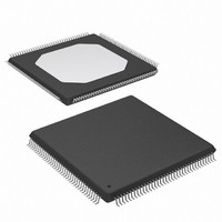
XC2S50E-6TQG144C Xilinx Inc, XC2S50E-6TQG144C Datasheet - Page 43

XC2S50E-6TQG144C
Manufacturer Part Number
XC2S50E-6TQG144C
Description
IC SPARTAN-IIE FPGA 50K 144-TQFP
Manufacturer
Xilinx Inc
Series
Spartan™-IIEr
Datasheet
1.XC2S50E-6TQG144C.pdf
(108 pages)
Specifications of XC2S50E-6TQG144C
Number Of Logic Elements/cells
1728
Number Of Labs/clbs
384
Total Ram Bits
32768
Number Of I /o
102
Number Of Gates
50000
Voltage - Supply
1.71 V ~ 1.89 V
Mounting Type
Surface Mount
Operating Temperature
0°C ~ 85°C
Package / Case
144-LQFP
Lead Free Status / RoHS Status
Lead free / RoHS Compliant
Other names
122-1331
Available stocks
Company
Part Number
Manufacturer
Quantity
Price
Company:
Part Number:
XC2S50E-6TQG144C
Manufacturer:
XILINX
Quantity:
1 450
Company:
Part Number:
XC2S50E-6TQG144C
Manufacturer:
XILINX
Quantity:
1 450
Company:
Part Number:
XC2S50E-6TQG144C
Manufacturer:
XILINX
Quantity:
151
Part Number:
XC2S50E-6TQG144C
Manufacturer:
TI/德州仪器
Quantity:
20 000
DLL Timing Parameters
Because of the difficulty in directly measuring many internal
timing parameters, those parameters are derived from
benchmark timing patterns. The following guidelines reflect
DLL Clock Tolerance, Jitter, and Phase Information
All DLL output jitter and phase specifications were deter-
mined through statistical measurement at the package pins
using a clock mirror configuration and matched drivers.
DS077-3 (v2.3) June 18, 2008
Product Specification
Notes:
1.
2.
3.
4.
5.
6.
T
Symbol
T
T
T
T
T
T
T
PHOOM
OJITCC
PHIOM
IJITCC
IPTOL
PHOO
LOCK
Commercial operating conditions. Add 30% for Industrial operating conditions.
Output Jitter is cycle-to-cycle jitter measured on the DLL output clock, excluding input clock jitter.
Phase Offset between CLKIN and CLKO is the worst-case fixed time difference between rising edges of CLKIN and CLKO,
excluding output jitter and input clock jitter.
Phase Offset between Clock Outputs on the DLL is the worst-case fixed time difference between rising edges of any two DLL
outputs, excluding output jitter and input clock jitter.
Maximum Phase Difference between CLKIN and CLKO is the sum of output jitter and phase offset between CLKIN and CLKO, or
the greatest difference between CLKIN and CLKO rising edges due to DLL alone (excluding input clock jitter).
Maximum Phase Difference between Clock Outputs on the DLL is the sum of output jitter and phase offset between any DLL
clock outputs, or the greatest difference between any two DLL output rising edges due to DLL alone (excluding input clock jitter).
PHIO
F
F
Symbol
T
CLKINHF
CLKINLF
DLLPW
R
Input clock period tolerance
Input clock jitter tolerance (cycle-to-cycle)
Time required for DLL to acquire lock
Output jitter (cycle-to-cycle) for any DLL clock output
Phase offset between CLKIN and CLKO
Phase offset between clock outputs on the DLL
Phase difference between CLKIN and CLKO
Phase difference between clock outputs on the DLL
Input clock frequency (CLKDLLHF)
Input clock frequency (CLKDLL)
Input clock pulse width
Description
Description
(1)
(3)
www.xilinx.com
Spartan-IIE FPGA Family: DC and Switching Characteristics
(5)
(4)
≥100 MHz
≥150 MHz
≥200 MHz
≥250 MHz
≥300 MHz
worst-case values across the recommended operating con-
ditions.
Figure 22, page
ters in the table below.
≥25 MHz
≥50 MHz
F
50-60 MHz
40-50 MHz
30-40 MHz
25-30 MHz
(6)
> 60 MHz
CLKIN
(2)
F
-
-
CLKIN
Min
5.0
3.0
2.4
2.0
1.8
1.5
1.3
60
25
44, provides definitions for various parame-
CLKDLLHF
Min
-
-
-
-
-
-
-
-
-
-
-
-
-7
Speed Grade
Max
320
160
-
-
-
-
-
-
-
±150
±100
±140
±160
± 200
Max
± 60
1.0
20
-
-
-
-
Min
5.0
3.0
2.4
2.0
1.8
1.5
NA
60
25
Min
CLKDLL
-
-
-
-
-
-
-
-
-
-
-
-
-6
± 300
± 200
±100
±140
±160
Max
Max
275
135
± 60
120
1.0
20
25
50
90
-
-
-
-
-
-
-
Units
Units
MHz
MHz
ns
ps
μs
μs
μs
μs
μs
ps
ps
ps
ps
ps
ns
ns
ns
ns
ns
ns
43


