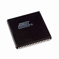
AT40K10-2AJC Atmel, AT40K10-2AJC Datasheet - Page 18

AT40K10-2AJC
Manufacturer Part Number
AT40K10-2AJC
Description
IC FPGA 576 CELL 84-PLCC
Manufacturer
Atmel
Series
AT40K/KLVr
Specifications of AT40K10-2AJC
Number Of Logic Elements/cells
576
Total Ram Bits
4608
Number Of I /o
62
Number Of Gates
20000
Voltage - Supply
4.75 V ~ 5.25 V
Mounting Type
Surface Mount
Operating Temperature
0°C ~ 70°C
Package / Case
84-PLCC
Lead Free Status / RoHS Status
Contains lead / RoHS non-compliant
Number Of Labs/clbs
-
Available stocks
Company
Part Number
Manufacturer
Quantity
Price
I/O Structure
PAD
PULL-UP/PULL-DOWN
TTL/CMOS
SCHMITT
DELAYS
DRIVE
TRI-STATE
SOURCE SELECTION MUX
18
AT40K/AT40KLV Series FPGA
The I/O pad is the one that connects the I/O to the outside world. Note that not all I/Os
have pads: the ones without pads are called Unbonded I/Os. The number of unbonded
I/Os varies with the device size and package. These unbonded I/Os are used to perform
a variety of bus turns at the edge of the array.
Each pad has a programmable pull-up and pull-down attached to it. This supplies a
weak “1” or “0” level to the pad pin. When all other drivers are off, this control will dictate
the signal level of the pad pin.
The input stage of each I/O cell has a number of parameters that can be programmed
either as properties in schematic entry or in the I/O Pad Attributes editor in IDS.
The threshold level can be set to either TTL/CMOS-compatible levels.
A Schmitt trigger circuit can be enabled on the inputs. The Schmitt trigger is a regenera-
tive comparator circuit that adds 1V hysteresis to the input. This effectively improves the
rise and fall times (leading and trailing edges) of the incoming signal and can be useful
for filtering out noise.
The input buffer can be programmed to include four different intrinsic delays as specified
in the AC timing characteristics. This feature is useful for meeting data hold require-
ments for the input signal.
The output drive capabilities of each I/O are programmable. They can be set to FAST,
MEDIUM or SLOW (using IDS tool). The FAST setting has the highest drive capability
(20 mA at 5V) buffer and the fastest slew rate. MEDIUM produces a medium drive
(14 mA at 5V) buffer, while SLOW yields a standard (6 mA at 5V) buffer.
The output of each I/O can be made tri-state (0, 1 or Z), open source (1 or Z) or open
drain (0 or Z) by programming an I/O’s Source Selection mux. Of course, the output can
be normal (0 or 1), as well.
The Source Selection mux selects the source for the output signal of an I/O, see
Figure 12 on page 20.
0896C–FPGA–04/02


