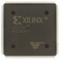
XCV100-5PQ240C Xilinx Inc, XCV100-5PQ240C Datasheet - Page 45

XCV100-5PQ240C
Manufacturer Part Number
XCV100-5PQ240C
Description
IC FPGA 2.5V 108K GATES 240-PQFP
Manufacturer
Xilinx Inc
Series
Virtex™r
Datasheet
1.XCV100-5PQ240C.pdf
(76 pages)
Specifications of XCV100-5PQ240C
Number Of Logic Elements/cells
2700
Number Of Labs/clbs
600
Total Ram Bits
40960
Number Of I /o
166
Number Of Gates
108904
Voltage - Supply
2.375 V ~ 2.625 V
Mounting Type
Surface Mount
Operating Temperature
0°C ~ 85°C
Package / Case
240-BFQFP
Lead Free Status / RoHS Status
Contains lead / RoHS non-compliant
Other names
122-1214
XCV100-5PQ240C
XCV100-5PQ240C
Available stocks
Company
Part Number
Manufacturer
Quantity
Price
DLL Timing Parameters
All devices are 100 percent functionally tested. Because of the difficulty in directly measuring many internal timing
parameters, those parameters are derived from benchmark timing patterns. The following guidelines reflect worst-case
values across the recommended operating conditions.
DLL Clock Tolerance, Jitter, and Phase Information
All DLL output jitter and phase specifications determined through statistical measurement at the package pins using a clock
mirror configuration and matched drivers.
DS003-3 (v3.2) September 10, 2002
Production Product Specification
Notes:
1.
Notes:
1.
2.
3.
4.
5.
6.
Input Clock Frequency (CLKDLLHF)
Input Clock Frequency (CLKDLL)
Input Clock Pulse Width (CLKDLLHF)
Input Clock Pulse Width (CLKDLL)
Input Clock Period Tolerance
Input Clock Jitter Tolerance (Cycle to Cycle)
Time Required for DLL to Acquire Lock
Output Jitter (cycle-to-cycle) for any DLL Clock Output
Phase Offset between CLKIN and CLKO
Phase Offset between Clock Outputs on the DLL
Maximum Phase Difference between CLKIN and
CLKO
Maximum Phase Difference between Clock Outputs on
the DLL
All specifications correspond to Commercial Operating Temperatures (0°C to + 85°C).
Output Jitter is cycle-to-cycle jitter measured on the DLL output clock, excluding input clock jitter.
Phase Offset between CLKIN and CLKO is the worst-case fixed time difference between rising edges of CLKIN and CLKO,
excluding Output Jitter and input clock jitter.
Phase Offset between Clock Outputs on the DLL is the worst-case fixed time difference between rising edges of any two DLL
outputs, excluding Output Jitter and input clock jitter.
Maximum Phase Difference between CLKIN an CLKO is the sum of Output Jitter and Phase Offset between CLKIN and CLKO,
or the greatest difference between CLKIN and CLKO rising edges due to DLL alone (excluding input clock jitter).
Maximum Phase DIfference between Clock Outputs on the DLL is the sum of Output JItter and Phase Offset between any DLL
clock outputs, or the greatest difference between any two DLL output rising edges sue to DLL alone (excluding input clock jitter).
All specifications correspond to Commercial Operating Temperatures (0°C to +85°C).
(4)
(5)
R
Description
Description
(2)
FCLKINHF
FCLKINLF
T
T
(3)
Symbol
DLLPWHF
DLLPWLF
www.xilinx.com
1-800-255-7778
(1)
Symbol
T
T
T
T
T
T
T
T
PHOOM
OJITCC
PHIOM
IJITCC
IPTOL
PHOO
LOCK
PHIO
Min
2.0
2.5
60
25
-6
50 - 60 MHz
40 - 50 MHz
30 - 40 MHz
25 - 30 MHz
Virtex™ 2.5 V Field Programmable Gate Arrays
> 60 MHz
Max
200
100
F
-
-
CLKIN
Speed Grade
Min
2.4
3.0
60
25
CLKDLLHF
Min
-5
-
-
-
-
-
-
-
Max
180
90
-
± 150
± 100
± 140
± 160
± 200
Max
± 60
1.0
20
-
-
-
-
Min
2.4
3.0
60
25
Min
CLKDLL
-
-
-
-
-
-
-
-4
Max
180
90
± 300
± 100
± 140
± 160
± 200
Max
± 60
-
-
120
1.0
20
25
50
90
Module 3 of 4
Units
MHz
MHz
Units
ns
ns
ns
ps
µs
µs
µs
µs
µs
ps
ps
ps
ps
ps
21


