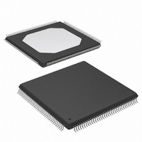
XCS20XL-4TQ144I Xilinx Inc, XCS20XL-4TQ144I Datasheet - Page 47

XCS20XL-4TQ144I
Manufacturer Part Number
XCS20XL-4TQ144I
Description
IC FPGA 3.3V I-TEMP HP 144TQFP
Manufacturer
Xilinx Inc
Series
Spartan™-XLr
Datasheet
1.XCS05XL-4VQG100C.pdf
(83 pages)
Specifications of XCS20XL-4TQ144I
Number Of Logic Elements/cells
950
Number Of Labs/clbs
400
Total Ram Bits
12800
Number Of I /o
113
Number Of Gates
20000
Voltage - Supply
3 V ~ 3.6 V
Mounting Type
Surface Mount
Operating Temperature
-40°C ~ 100°C
Package / Case
144-LQFP
Lead Free Status / RoHS Status
Contains lead / RoHS non-compliant
Available stocks
Company
Part Number
Manufacturer
Quantity
Price
Company:
Part Number:
XCS20XL-4TQ144I
Manufacturer:
XILINX
Quantity:
252
Part Number:
XCS20XL-4TQ144I
Manufacturer:
XILINX/赛灵思
Quantity:
20 000
Spartan Family Pin-to-Pin Output Parameter Guidelines
All devices are 100% functionally tested. Pin-to-pin timing
parameters are derived from measuring external and inter-
nal test patterns and are guaranteed over worst-case oper-
ating conditions (supply voltage and junction temperature).
Listed below are representative values for typical pin loca-
tions and normal clock loading. For more specific, more pre-
Spartan Family Output Flip-Flop, Clock-to-Out
DS060 (v1.8) June 26, 2008
Product Specification
Notes:
1.
2.
3.
Global Primary Clock to TTL Output using OFF
Global Secondary Clock to TTL Output using OFF
Delay Adder for CMOS Outputs Option
T
Symbol
T
T
T
T
CMOSOF
T
CMOSO
ICKSOF
ICKOF
ICKSO
ICKO
Listed above are representative values where one global clock input drives one vertical clock line in each accessible column,and
where all accessible IOB and CLB flip-flops are clocked by the global clock net.
Output timing is measured at ~50% V
OFF = Output Flip-Flop
R
Fast
Slew-rate limited
Fast
Slew-rate limited
Fast
Slew-rate limited
Description
CC
threshold with 50 pF external capacitive load. For different loads, see
www.xilinx.com
cise, and worst-case guaranteed data, reflecting the actual
routing structure, use the values provided by the static tim-
ing analyzer (TRCE in the Xilinx Development System) and
back-annotated to the simulation netlist. These path delays,
provided as a guideline, have been extracted from the static
timing analyzer report.
Spartan and Spartan-XL FPGA Families Data Sheet
All devices
All devices
Device
XCS05
XCS10
XCS20
XCS30
XCS40
XCS05
XCS10
XCS20
XCS30
XCS40
XCS05
XCS10
XCS20
XCS30
XCS40
XCS05
XCS10
XCS20
XCS30
XCS40
Max
10.2
10.5
10.3
10.7
11.0
5.3
5.7
6.1
6.5
6.8
9.0
9.4
9.8
5.8
6.2
6.6
7.0
7.3
9.5
9.9
0.8
1.5
-4
Speed Grade
Figure
Max
10.2
11.5
12.0
12.2
12.8
12.8
10.7
12.0
12.5
12.7
13.2
14.3
8.7
9.1
9.3
9.4
9.2
9.6
9.8
9.9
1.0
2.0
-3
33.
Units
ns
ns
ns
ns
ns
ns
ns
ns
ns
ns
ns
ns
ns
ns
ns
ns
ns
ns
ns
ns
ns
ns
47


