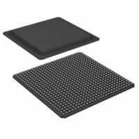
XC2V3000-6FGG676C Xilinx Inc, XC2V3000-6FGG676C Datasheet - Page 3

XC2V3000-6FGG676C
Manufacturer Part Number
XC2V3000-6FGG676C
Description
IC FPGA VIRTEX-II 3M 676-FBGA
Manufacturer
Xilinx Inc
Series
Virtex™-IIr
Datasheet
1.XC2V250-4FGG256C.pdf
(318 pages)
Specifications of XC2V3000-6FGG676C
Number Of Labs/clbs
3584
Total Ram Bits
1769472
Number Of I /o
484
Number Of Gates
3000000
Voltage - Supply
1.425 V ~ 1.575 V
Mounting Type
Surface Mount
Operating Temperature
0°C ~ 85°C
Package / Case
676-BBGA
Lead Free Status / RoHS Status
Lead free / RoHS Compliant
Number Of Logic Elements/cells
-
Available stocks
Company
Part Number
Manufacturer
Quantity
Price
Company:
Part Number:
XC2V3000-6FGG676C
Manufacturer:
Xilinx Inc
Quantity:
10 000
- Current page: 3 of 318
- Download datasheet (3Mb)
Table 1: Virtex-II Field-Programmable Gate Array Family Members
General Description
The Virtex-II family is a platform FPGA developed for high
performance from low-density to high-density designs that
are based on IP cores and customized modules. The family
delivers complete solutions for telecommunication, wire-
less, networking, video, and DSP applications, including
PCI, LVDS, and DDR interfaces.
The leading-edge 0.15 µm / 0.12 µm CMOS 8-layer metal
process and the Virtex-II architecture are optimized for high
speed with low power consumption. Combining a wide vari-
ety of flexible features and a large range of densities up to
10 million system gates, the Virtex-II family enhances pro-
grammable logic design capabilities and is a powerful alter-
native to mask-programmed gates arrays. As shown in
Table
from 40K to 8M system gates.
Packaging
Offerings include ball grid array (BGA) packages with
0.80 mm, 1.00 mm, and 1.27 mm pitches. In addition to tra-
ditional wire-bond interconnects, flip-chip interconnect is
used in some of the BGA offerings. The use of flip-chip
interconnect offers more I/Os than is possible in wire-bond
versions of the similar packages. Flip-chip construction
offers the combination of high pin count with high thermal
capacity.
DS031-1 (v3.5) November 5, 2007
Product Specification
Notes:
1. See details in
XC2V40
XC2V80
XC2V250
XC2V500
XC2V1000
XC2V1500
XC2V2000
XC2V3000
XC2V4000
XC2V6000
XC2V8000
Device
1, the Virtex-II family comprises 11 members, ranging
R
System
Gates
Table 2, “Maximum Number of User I/O Pads”
250K
500K
1.5M
40K
80K
1M
2M
3M
4M
6M
8M
Row x Col.
112 x 104
(1 CLB = 4 slices = Max 128 bits)
24 x 16
32 x 24
40 x 32
48 x 40
56 x 48
64 x 56
80 x 72
96 x 88
16 x 8
Array
8 x 8
10,752
14,336
23,040
33,792
46,592
Slices
1,536
3,072
5,120
7,680
CLB
256
512
Distributed
RAM Kbits
Maximum
www.xilinx.com
1,056
1,456
160
240
336
448
720
16
48
96
8
.
Wire-bond packages CS, FG, and BG are optionally avail-
abe in Pb-free versions CSG, FGG, and BGG. See
Ordering Examples, page
Table 2
The Virtex-II device/package combination table
the end of this section) details the maximum number of I/Os
for each device and package using wire-bond or flip-chip
technology.
Table 2: Maximum Number of User I/O Pads
XC2V40
XC2V80
XC2V250
XC2V500
XC2V1000
XC2V1500
XC2V2000
XC2V3000
XC2V4000
XC2V6000
XC2V8000
Virtex-II Platform FPGAs: Introduction and Overview
Multiplier
Blocks
120
144
168
24
32
40
48
56
96
Device
4
8
shows the maximum number of user I/Os available.
18 Kbit
Blocks
SelectRAM Blocks
120
144
168
24
32
40
48
56
96
4
8
Wire-Bond
6.
Max RAM
(Kbits)
120
200
264
328
392
516
1,008
1,728
2,160
2,592
3,024
88
144
432
576
720
864
-
-
-
-
72
DCMs
12
12
12
12
4
4
8
8
8
8
8
Flip-Chip
Module 1 of 4
1,104
1,108
432
528
624
720
912
(Table 6
-
-
-
-
Max I/O
Pads
1,104
1,108
Virtex-II
120
200
264
432
528
624
720
912
88
(1)
at
2
Related parts for XC2V3000-6FGG676C
Image
Part Number
Description
Manufacturer
Datasheet
Request
R

Part Number:
Description:
IC VIRTEX-II FPGA 3M 676-FBGA
Manufacturer:
Xilinx Inc
Datasheet:

Part Number:
Description:
IC VIRTEX-II FPGA 3M 1152-FCBGA
Manufacturer:
Xilinx Inc
Datasheet:

Part Number:
Description:
IC FPGA VIRTEX II 3M 957-FCBGA
Manufacturer:
Xilinx Inc
Datasheet:

Part Number:
Description:
IC FPGA VIRTEX-II 3M 676-FBGA
Manufacturer:
Xilinx Inc
Datasheet:

Part Number:
Description:
IC FPGA VIRTEX II 3M 957-FCBGA
Manufacturer:
Xilinx Inc
Datasheet:

Part Number:
Description:
IC FPGA VIRTEX-II 3M 1152-FBGA
Manufacturer:
Xilinx Inc
Datasheet:

Part Number:
Description:
IC FPGA VIRTEX-II 3M 1152-FBGA
Manufacturer:
Xilinx Inc
Datasheet:

Part Number:
Description:
IC FPGA VIRTEX-II 3M 676-FBGA
Manufacturer:
Xilinx Inc
Datasheet:

Part Number:
Description:
IC FPGA VIRTEX-II 3M 1152-FBGA
Manufacturer:
Xilinx Inc
Datasheet:

Part Number:
Description:
IC FPGA VIRTEX-II 3M 1152-FBGA
Manufacturer:
Xilinx Inc
Datasheet:

Part Number:
Description:
IC FPGA VIRTEX-II 676FGBGA
Manufacturer:
Xilinx Inc
Datasheet:

Part Number:
Description:
IC FPGA VIRTEX-II 728PBGA
Manufacturer:
Xilinx Inc
Datasheet:

Part Number:
Description:
IC FPGA VIRTEX-II 1152FCBGA
Manufacturer:
Xilinx Inc
Datasheet:

Part Number:
Description:
IC FPGA VIRTEX-II 957FCBGA
Manufacturer:
Xilinx Inc
Datasheet:

Part Number:
Description:
IC FPGA VIRTEX-II 957FCBGA
Manufacturer:
Xilinx Inc
Datasheet:


