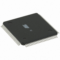
AT40K05-2AQC Atmel, AT40K05-2AQC Datasheet - Page 8

AT40K05-2AQC
Manufacturer Part Number
AT40K05-2AQC
Description
IC FPGA 5K GATES 100TQFP
Manufacturer
Atmel
Series
AT40K/KLVr
Specifications of AT40K05-2AQC
Number Of Logic Elements/cells
256
Total Ram Bits
2048
Number Of I /o
78
Number Of Gates
10000
Voltage - Supply
4.75 V ~ 5.25 V
Mounting Type
Surface Mount
Operating Temperature
0°C ~ 70°C
Package / Case
100-TFQFP
Lead Free Status / RoHS Status
Contains lead / RoHS non-compliant
Number Of Labs/clbs
-
Other names
AT40K052AQC
Available stocks
Company
Part Number
Manufacturer
Quantity
Price
Cell Connections
The Cell
8
AT40K/AT40KLV Series FPGA
Figure 4(a) depicts direct connections between a cell and its eight nearest neighbors.
Figure 4(b) shows the connections between a cell and five horizontal local buses (1 per
busing plane) and five vertical local buses (1 per busing plane).
Figure 4. Cell Connections
Figure 5 depicts the AT40K/AT40KLV cell. Configuration bits for separate muxes and
pass gates are independent. All permutations of programmable muxes and pass gates
are legal. V
connected to the horizontal local bus in plane n . A local/local turn in plane n is achieved
by turning on the two pass gates connected to V
signals into the cell from a local bus or to drive a signal out onto a local bus. Signals
coming into the logic cell on one local bus plane can be switched onto another plane by
opening two of the pass gates. This allows bus signals to switch planes to achieve
greater route ability. Up to five simultaneous local/local turns are possible.
The AT40K/AT40KLV FPGA core cell is a highly configurable logic block based around
two 3-input LUTs (8 x 1 ROM), which can be combined to produce one 4-input LUT.
This means that any core cell can implement two functions of 3 inputs or one function of
4 inputs. There is a Set/Reset D flip-flop in every cell, the output of which may be tri-
stated and fed back internally within the core cell. There is also a 2-to-1 multiplexer in
every cell, and an upstream AND gate in the “front end” of the cell. This AND gate is an
important feature in the implementation of efficient array multipliers.
With this functionality in each core cell, the core cell can be configured in several
“modes”. The core cell flexibility makes the AT40K/AT40KLV architecture well suited to
most digital design application areas, see Figure 6.
CELL
CELL
CELL
n
(a) Cell-to-cell Connections
(V
1
- V
5
) is connected to the vertical local bus in plane n. H
CELL
CELL
CELL
Direct Connect
Orthogonal
Direct Connect
CELL
CELL
CELL
Diagonal
n
Plane 5
Plane 4
Plane 3
Plane 2
Plane 1
and H
(b) Cell-to-bus Connections
n
Busing Plane
. Pass gates are opened to let
Vertical
W
X
Y
Z
L
WXYZL
CELL
0896C–FPGA–04/02
n
(H
Horizontal
Busing Plane
1
- H
5
) is


