20-101-0356 Rabbit Semiconductor, 20-101-0356 Datasheet
20-101-0356
Specifications of 20-101-0356


Related parts for 20-101-0356


20-101-0356 Summary of contents
Page 1
... Jackrabbit (BL1800) C-Programmable Single-Board Computer User’s Manual 019–0067 • 090515–J ...
Page 2
... Digi International reserves the right to make changes and improvements to its products without providing notice. Rabbit and Dynamic C are registered trademarks of Digi International Inc. Rabbit 2000 is a trademark of Digi International Inc. The latest revision of this manual is available on the Rabbit Web site, www.rabbit.com, for free, unregistered download. ...
Page 3
... Real-Time Clock .........................................................................................................................14 2.5.2 Technical Support .......................................................................................................................14 Chapter 3. Subsystems 3.1 Jackrabbit Pinouts ...............................................................................................................................16 3.1.1 Headers........................................................................................................................................16 3.2 Digital Inputs/Outputs.........................................................................................................................17 3.2.1 Digital Inputs...............................................................................................................................17 3.2.2 Digital Outputs............................................................................................................................18 3.2.3 Bidirectional I/O .........................................................................................................................20 3.3 A/D Converter.....................................................................................................................................21 3.4 D/A Converters ...................................................................................................................................23 3.4.1 DA1 .............................................................................................................................................24 3.4.2 DA0 .............................................................................................................................................26 3.5 Serial Communication ........................................................................................................................28 3.5.1 RS-232 ........................................................................................................................................28 3.5.2 RS-485 ........................................................................................................................................28 3 ...
Page 4
... A.1 Electrical and Mechanical Specifications.......................................................................................... 58 A.1.1 Exclusion Zone .......................................................................................................................... 60 A.1.2 Headers ...................................................................................................................................... 61 A.2 Jumper Configurations ...................................................................................................................... 62 A.3 Conformal Coating ............................................................................................................................ 64 A.4 Use of Rabbit 2000 Parallel Ports ..................................................................................................... 65 Appendix B. Prototyping Board B.1 Prototyping Board Overview............................................................................................................. 70 B.1.1 Prototyping Board Features ....................................................................................................... 71 B.2 Mechanical Dimensions and Layout ................................................................................................. 72 B.3 Using the Prototyping Board ............................................................................................................. 73 B ...
Page 5
... CMOS-compatible I/O • 3 analog channels: 1 A/D input, 2 PWM D/A outputs • 4 high-power outputs (factory-configured as 3 sinking and 1 sourcing) • 4 serial ports (2 RS-232 or 1 RS-232 with RTS/CTS, 1 RS-485, and 1 CMOS- compatible) • 6 timers (five 8-bit timers and one 10-bit timer) • 128K SRAM, 256K flash EPROM • ...
Page 6
... Visit the Web site for up-to-date information about additional add-ons and features as they become available. The Web site also has the latest revision of this user’s manual. 1.2 Development and Evaluation Tools A complete Development Kit, including a Prototyping Board and Dynamic C develop- ment software, is available for the Jackrabbit ...
Page 7
... How to Use This Manual This user’s manual is intended to give users detailed information on the Jackrabbit. It does not contain detailed information on the Dynamic C development environment or the Rabbit ® 2000 microprocessor. Most users will want more detailed information on some or all of these topics in order to put the Jackrabbit to effective use. ...
Page 8
... These limits apply over the range of 30–230 MHz. The limits are 7 dB higher for frequen- cies above 230 MHz. Although the test range goes to 1 GHz, the emissions from Rabbit- based systems at frequencies above 300 MHz are generally well below background noise levels ...
Page 9
... When connecting the Jackrabbit single-board computer to outdoor cables, the customer is responsible for providing CE-approved surge/lightning protection. • Rabbit recommends placing digital I/O or analog cables that are longer in a metal conduit to assist in maintaining CE compliance and to conform to good cable design practices. Rabbit also recommends using properly shielded I/O cables in noisy electromagnetic environments. • ...
Page 10
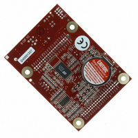
Jackrabbit (BL1800) ...
Page 11
... The Jackrabbit Development Kit contains the following items: • BL1810 single-board computer. • Prototyping Board. • Universal AC adapter DC (includes Canada/Japan/U.S., Australia/N.Z., U.K., and European style plugs). If you are using another power supply, it must provide 7.5– The linear voltage regulator becomes rather hot for voltages above 15 V. ...
Page 12
Development Hardware Connections There are three steps to connecting the Prototyping Board for use with Dynamic C and the sample programs: 1. Attach the Jackrabbit to the Prototyping Board. 2. Connect the programming cable between the Jackrabbit and the ...
Page 13
... Board. The header pins may become bent or damaged if the pin alignment is offset, and the Jackrabbit might not work. Permanent electrical damage to the may also result if a misaligned Jackrabbit is powered up. Press the Jackrabbit’s pins firmly into the Prototyping Board headers. User’s Manual + ...
Page 14
... NOTE: Use only the programming cable that has a red shrink wrap around the RS-232 level converter (Part No. 20-101-0513), which is supplied with the Development Kit. Other Rabbit programming cables are not voltage-compatible or their connector sizes may be different. ...
Page 15
... To power down the Jackrabbit, unplug the power connector from J1. You should discon- nect power before making any circuit adjustments in the prototyping area, changing any connections to the board, or removing the Jackrabbit from the Prototyping Board. User’s Manual 11 ...
Page 16
... The online documentation is installed along with Dynamic C, and an icon for the docu- mentation menu is placed on the workstation’s desktop. Double-click this icon to reach the menu. If the icon is missing, create a new desktop icon that points to folder, found in the Dynamic C installation folder. ...
Page 17
... If Dynamic C cannot find the target system (error message ): Detected." • Check that the BL1810 is powered correctly — the AC adapter should be connected to header J1 on the Jackrabbit board • Check both ends of the programming cable to ensure that they are firmly plugged into ...
Page 18
... Dynamic C installation folder. default.htm docs 3. For advanced development topics, refer to the Dynamic C User’s Manual, also in the online documentation set. 2.5.1 Real-Time Clock If you plan to use the real-time clock functionality in your application, you will need to set the real-time clock. You may set the real-time clock using the ...
Page 19
... Chapter 3 describes the principal subsystems and their use for the Jackrabbit. • Digital Inputs/Outputs • A/D Converter • D/A Converters • Serial Communication • Memory Figure 3 shows these Rabbit-based subsystems designed into the Jackrabbit. Figure 3. Jackrabbit Subsystems User’s Manual 3. S UBSYSTEMS ...
Page 20
... Jackrabbit Pinouts Figure 4 shows the pinout for headers J4 and J5, which carry the signals associated with the Jackrabbit subsystems. Figure 4. Pinout for Jackrabbit Headers J4 and J5 3.1.1 Headers Standard Jackrabbit models are equipped with two 2 × 20 IDC headers (J4 and J5) with pitch. 16 Jackrabbit (BL1800) ...
Page 21
... Digital Inputs The Jackrabbit has six CMOS-level digital inputs, PB0–PB5, each of which is pulled shown in Figure 5. The BL1820, which does not have RS-485, has one additional CMOS-level digital input, PC1. The actual switching threshold is approximately 2.40 V. Anything below this value is a ...
Page 22
... The Jackrabbit has four CMOS-level digital outputs, PB6–PB7, PCLK, and IOBEN. Four high-power outputs, HV0–HV3, are also available—HV0–HV2 can each sink (200 mA for the BL1810 and BL1820 and HV3 can source up to 500 mA (100 mA for the BL1810 and BL1820 The BL1820, which does not have RS-485, has one additional CMOS-level digital output, PC0 ...
Page 23
... W Figure 7. Configurable High-Current Output When used as a sourcing output, HV3 is switched to K when PE3 on the Rabbit 2000 goes high, and the two transistors shown in Figure 7 are turned on. The maximum sourcing cur- rent is 100 mA (BL1810 and BL1820) or 500 mA (BL1800), and the maximum ...
Page 24
... Figure 8. Changing HV3 to a Sinking Output 3.2.3 Bidirectional I/O The Jackrabbit has 14 CMOS-level bidirectional I/O: PA0–PA7, PD0, PD3, PD6–PD7, and PE4–PE5. The BL1820, which does not have RS-485, has one additional bidirectional I/O, PD5. 20 Jackrabbit (BL1800) ...
Page 25
... A/D input is exactly the same as DA0. If AD0 < 1.990 V, PE7 would read low and PE6 would read high. PE6 can be imagined “DA0 voltage is too high” indicator. If DA0 is larger than the analog voltage presented at AD0, then PE6 will be true (high). If this happens, the pro- gram will need to reduce the DA0 voltage. PE7 can be imagined “ ...
Page 26
... This is because Vcc can vary ±5%, the pulse-width modulated outputs might not reach the full 0 V and 5 V rails out of the Rabbit 2000 micro- processor, and the gain resistors used in the circuit have a 1% tolerance. For these reasons, each Jackrabbit needs to be calibrated individually, with the constants held in software able to rely on an absolute accuracy ...
Page 27
... V. If the time only 25% of the time, then the average voltage will be 1.25 V. Thus, the software needs to only vary the time the signal with respect to the time the signal achieve any desired voltage between 0 V and 5 V. User’s Manual W W ...
Page 28
... DA1 output depends on the smallest increment of time to change the on/off time (the time between 5 V and 0 V). The Jackrabbit uses the Rabbit 2000’s Port D control reg- isters to clock out the signal at a timer timeout. The timer used is timer B. Timer B has 10 bits of resolution so that the voltage can be varied in 1/1024 increments ...
Page 29
... Below 1 V, the D/A converter can only sink a maxi- mum of 100 µA. To summarize, DA1 is provided uncalibrated, can be programmed with a resolution and a peak-to-peak ripple less than 20 mV over the range from 0 3.5 V and 0 V. The settling time to within ms. User’s Manual ...
Page 30
... It is important to remember that the DA0 output voltage will not be realized instantaneously after programming in a value. There is a settling time because of the RC time constant (R21 || R27 × C20), which is 7.68 ms. For example, the voltage at any given time is where V is the voltage at time t, V put voltage from the D/A converter, and RC is the time constant (7 ...
Page 31
... The resolution of the DA0 output depends on the smallest increment of time to change the on/off time (the time between 5 V and 0 V). The Jackrabbit uses the Rabbit 2000’s Port D control registers to clock out the signal at a timer timeout. The timer used is timer B. ...
Page 32
... RS-232 serial communication protocol. Basically, the chip translates the Rabbit 2000’ +Vcc signals to ±10 V. Note that the polarity is reversed in an RS-232 circuit so that + output as –10 V and output as + also provides the proper line loading for reliable communication. ...
Page 33
... Figure 11. Multidrop Jackrabbit Network User’s Manual 29 ...
Page 34
... When using more than 10 Jackrabbits in a multidrop network, leave the 681 Ω bias resistors in place on the master Jackrabbit, and leave the 220 Ω termination resistors in place on the Jackrabbit at each end of the network. 3.5.3 Programming Port The Jackrabbit has a 10-pin program header labeled J3. The programming port uses the Rabbit 2000’ ...
Page 35
... It can be driven low during an interrupt acknowledge cycle can also serve as a general-purpose output. The /RESET_IN pin is an external input that is used to reset the Rabbit 2000 and the onboard peripheral circuits on the RabbitCore module. The serial programming port can be used to force a hard reset on the RabbitCore module by asserting the /RESET_IN signal. ...
Page 36
... When the Rabbit 2000 is reset, the operating mode is determined by the status of the SMODE pins. When the programming cable’s connector is attached, the SMODE pins are pulled high, placing the Rabbit 2000 in the Program Mode. When the programming cable’s SMODE pins are pulled low, causing the Rabbit 2000 to operate in the Run Mode ...
Page 37
... Standard Jackrabbit models come with 128K of SRAM. A factory-installed option for 512K of SRAM is available. Figure 14 shows the locations and the jumper settings for the jump- ers at JP1 used to set the SRAM size. The “jumpers” are 0 Ω surface-mounted resistors. Figure 14. Jackrabbit Jumper Settings for SRAM Size NOTE: For ordering or other information involving the factory-installed 512K SRAM option, call your Rabbit sales representative or distributor ...
Page 38
... Clock Doubler Jackrabbit BL1810 and BL1820 models take advantage of the Rabbit 2000 microproces- sor’s internal clock doubler. A built-in clock doubler allows half-frequency crystals to be used to reduce radiated emissions. The 14.74 MHz frequency is generated using a 7.37 MHz resonator. The clock doubler is disabled automatically in the BIOS for crystals or resonators with a frequency above 12 ...
Page 39
... Spectrum Spreader Jackrabbit boards that carry the CE mark have a Rabbit 2000 microprocessor that features a spectrum spreader, which helps to mitigate EMI problems. By default, the spectrum spreader is on automatically for Jackrabbit BL1810 and BL1820 boards that carry the CE mark when used with Dynamic C 7.32 or later versions, but the spectrum spreader may also be turned off or set to a stronger setting ...
Page 40
Jackrabbit (BL1800) ...
Page 41
... Dynamic C development environment. Debugging occurs while the application runs on the target. Alternatively, users can compile a program to an image file for later loading. Dynamic C runs on PCs under Windows NT and later— note that Dynamic C is still being evaluated for compatibility with Windows Vista at the time of writing, and should not be expected to run correctly under Windows Vista at this time ...
Page 42
... Standard debugging features: Breakpoints—Set breakpoints that can disable interrupts. Single-stepping—Step into or over functions at a source or machine code level, µC/OS-II aware. Code disassembly—The disassembly window displays addresses, opcodes, mnemonics, and machine cycle times. Switch between debugging at machine-code level and source-code level by simply opening or closing the disassembly window. Watch expressions— ...
Page 43
... Program Mode (programming cable is attached to programming port as shown in Figure 2) and must be connected using the programming cable. More complete information on Dynamic C is provided in the Dynamic C User’s Manual. The sample programs are listed in Table 4. Table 4. Jackrabbit Sample Programs The first five sample programs provide a step-by-step introduction to the Jackrabbit board. ...
Page 44
... F9 should start flashing if everything went well. If this doesn’t work review the following points. • The target should be ready, which is indicated by the message “BIOS successfully com- piled...” If you did not receive this message or you get a communication error, recom- pile the BIOS by typing < ...
Page 45
... If the “BIOS successfully compiled …” message does not display, try a different serial port using the Dynamic C plugged into. Don’t change anything in this menu except the COM number. The baud rate should be 115,200 bps and the stop bits should be 1. ...
Page 46
... Summary of Features So far you have practiced using the following features of Dynamic C. • Loading, compiling and running a program. When you load a program it appears in an edit window. You can compile by selecting menu. When you compile the program compiled into machine language Compile and downloaded to the target over the serial port ...
Page 47
... This will cause the program to break if the execution thread hits your break point. • Watch expressions. A watch expression expression that is evaluated on command in the watch window. An expression is basically any type of C formula that can include operators, variables and function calls, but not statements that require multiple lines such as for or switch ...
Page 48
... The pins on Parallel Port A can all be set as either outputs or as inputs via the slave port control register (SPCTR). Do not use Parallel Port A if the slave port is being used. Bits 0–5 on Parallel Port B are always inputs, and bits 6–7 are always outputs. Do not use Parallel Port B if the slave port is being used. ...
Page 49
... This sample program only involves writing, and that is why we ground the R/W pin. VEE is used to control brightness—the simplest thing ground it. If you need to control the brightness, you can connect a potentiometer between ground and -5 V, with the arm going to the VEE pin ...
Page 50
... JR_FLOWCONTROL.C uring Serial Port C (PC3/PC2) for CTS/RTS with serial data coming from TxB at 115,200 bps. One character at a time is received and is displayed in the To set up the Prototyping Board, you will need to tie PC4 and PC5 (TxB and RxB) together at header J1, and you will also tie PC2 and PC3 (TxC and RxC) together as shown in the diagram ...
Page 51
... NOTE: If your version of Dynamic C is earlier than 6.55, see Technical Note 117, Jack- rabbit (BL1800 Series) RS-485 Bulletin, for information on restrictions on using both DA1 and RS-485 at the same time. User’s Manual 15 // Send Alphabet // Wait for Echo // Wait for Reply ...
Page 52
... Dynamic C has language extensions to support multitasking. The major C constructs are called costatements, cofunctions, and slicing. These are described more completely in the Dynamic C User’s Manual. The example below, sample program tatements. A costatement is a way to perform a sequence of operations that involve pauses or waits for some external event to take place. A complete description of costatements is in the Dynamic C User’ ...
Page 53
... S1 main(){ WrPortI(SPCR,NULL,0x84); WrPortI(PADR,&PADRShadow,0xff); vswitch=0; (1) while (1) { BigLoopTop(); // first task flash LED DS4 every second for 200 milliseconds (2) costate { BitWrPortI(PADR,&PADRShadow,0,3); // LED DS4 on (3) waitfor(DelayMs(200)); BitWrPortI(PADR,&PADRShadow,1,3); // LED DS4 off waitfor(DelayMs(800)); ( second task - debounce switch #1 and toggle virtual switch vswitch ...
Page 54
... At (6) a use for a shadow register is illustrated. A shadow register is used to keep track of the contents of an I/O port that is write only - it can’t be read back. If every time a write is made to the port the same bits are set in the shadow register, then the shadow register has the same data as the port register ...
Page 55
... The function void jrioInit() sets up parallel port D bits 1, 2, and 4 for analog output, port E bits 0–3 for digital output, and starts up the pulse-width modulation routines for the A/D and D/A channels. Note that these routines can consume up to 20% of the CPU’s processing power; the routines use timer B and the B1 and B2 match registers ...
Page 56
... The output channels can also be set in an “always on” or “always off” mode, which does not require CPU cycles. The “always on” mode is set by requesting an output value of 1024, and will provide about 3 channel DA0, and 3 DA1. The “always off” mode is selected by asking for a value of 0, and provides an output of around 0 DA0 and 0 ...
Page 57
... Jackrabbit). value is an integer from 0–1024 that corresponds to an output voltage as shown in Table 5. NOTE: See the sample program JRIOTEST.C for examples of using the anaOut func- tion. Effect of Interrupts on Analog I/O The stability of the voltage output (and hence the voltage input determination as well) depends on the ability of the driver to respond quickly to interrupt requests ...
Page 58
... The parameters are identical to those described above for NOTE: See sample program JRIO_COF.C for an example of the use of cof_anaIn – V max min = -------------------------------------------------------------------- - PWM_MAX0 PWM_MIN – × voltage = m value + b for DA0 to provide that same voltage). anaOut(0,value) , corresponding to a voltage value anaIn ...
Page 59
... Enable high for pins 6 and 7 to act as outputs, and low for those pins to act as inputs. Parallel Ports D and E on the Rabbit 2000 are double-buffered to provide precisely timed updating of the output pins. Each port is divided into an upper and a lower nibble. All bits of each nibble must be updated simultaneously ...
Page 60
Upgrading Dynamic C 4.5.1 Patches and Bug Fixes Dynamic C patches that focus on bug fixes are available from time to time. Check the Web site www.rabbit.com/support/ The default installation of a patch or bug fix is to install ...
Page 61
... A Appendix A provides the specifications for the Jackrabbit. User’s Manual A. S PPENDIX PECIFICATIONS 57 ...
Page 62
A.1 Electrical and Mechanical Specifications Figure A-1 shows the mechanical dimensions for the Jackrabbit. Figure A-1. Jackrabbit Dimensions NOTE: All measurements are in inches followed by millimeters enclosed in parentheses. All dimensions have a manufacturing tolerance of ±0.01" (0.25 mm). ...
Page 63
... Analog Outputs Up to four serial ports: • two RS-232 or one RS-232 (with CTS/RTS) rated ESD • Serial Ports one RS-485 rated ESD (RS-485 driver not installed on BL1820) • one 5 V CMOS-compatible programming port Two serial ports (A and B) can be clocked. Serial Rate Connectors ...
Page 64
... It is recommended that you allow for “exclusion zones” around the Jackrabbit when the Jackrabbit is incorporated into an assembly that includes other components. These “exclu- sion zones” that you keep free of other components and boards will allow for sufficient air flow, and will help to minimize any electrical or EMI interference between adjacent boards. Figure A-2 shows the “ ...
Page 65
... The Jackrabbit has 0.1" IDC headers × 3) and J2 (2 × 2) for the power supply and an external battery connection. There are 2 mm IDC headers × 5 programming port) and at J4 and J5 (2 × 20 Rabbit subsystems) for physical connection to other boards or ribbon cables. Figure A-3 shows the Jackrabbit footprint to help you lay out the “motherboard” into which the Jackrabbit is plugged in ...
Page 66
A.2 Jumper Configurations Figure A-4 shows the header and jumper locations used to configure the various Jackrabbit options. Figure A-4. Location of Jackrabbit Configurable Positions 62 Jackrabbit (BL1800) ...
Page 67
... Flash Memory Bank Select — HV3 Sinking/Sourcing RS-485 Bias and Termination — Resistors (not installed on BL1820) NOTE: Header JP3 is available only on Jackrabbit boards labeled 175-0255. These boards were introduced in 2003. User’s Manual Pins Connected n.c. 32K 1–2 128K 2–3 512K 1–2 128K/256K 2– ...
Page 68
... A.3 Conformal Coating The areas around the crystal oscillator and the battery backup circuit on the Jackrabbit have had the Dow Corning silicone-based 1-2620 conformal coating applied. The confor- mally coated areas are shown in Figure A-5. The conformal coating protects these high- impedance circuits from the effects of moisture and contaminants over time, and helps to maintain the accuracy of the real-time clock ...
Page 69
... A.4 Use of Rabbit 2000 Parallel Ports Figure A-6 shows the use of the Rabbit 2000 parallel ports. The Jackrabbit has 27 general- purpose digital inputs/outputs available on headers J4 and J5—15 are bidirectional (one of which is used by the RS-485 chip on BL1800 and BL1810 models), seven are inputs only ...
Page 70
... The ports on the Rabbit 2000 microprocessor used in the Jackrabbit are configurable, and so the factory defaults can be reconfigured. Table A-3 lists the Rabbit 2000 factory defaults and the alternate configurations. Table A-3. Jackrabbit Pinout Configurations Rabbit 2000 Pin Factory Default PA0–PA7 Parallel I/O ...
Page 71
... As shown in Table A-3, pins PE4 and PE5 can instead be used as external INT0B and INT1B interrupts. Pins PD6 and PD7 can instead be used to access Serial Port A on the Rabbit 2000 microprocessor. Pins PB0 and PB1 can instead be used to access the clock on Serial Port B and Serial Port A of the Rabbit 2000 microprocessor. ...
Page 72
Jackrabbit (BL1800) ...
Page 73
... A PPENDIX Appendix B describes the features and accessories of the Proto- typing Board, and explains the use of the Prototyping Board to demonstrate the Jackrabbit and to build prototypes of your own circuits. User’s Manual B. P ROTOTYPING B OARD 69 ...
Page 74
B.1 Prototyping Board Overview The Prototyping Board included in the Development Kit makes it easy to connect a Jack- rabbit board to a power supply and a PC workstation for development. It also provides some basic I/O peripherals (switches and ...
Page 75
... PB2–PB5 pins of the Rabbit 2000 microprocessor on the Jackrabbit, and may be read as inputs by sample applications. Four LEDs are connected to the PA1–PA4 pins of the of the Rabbit 2000 microproces- sor on the Jackrabbit, and may be driven as output indicators by sample applications. Prototyping Area — ...
Page 76
B.2 Mechanical Dimensions and Layout Figure B-2 shows the mechanical dimensions and layout for the Jackrabbit Prototyping Board. Figure B-2. Jackrabbit Prototyping Board 72 Jackrabbit (BL1800) ...
Page 77
... Getting Started Manual, solder the headers included in the bag of spare parts onto the Prototyping Board. Solder a 10-pin header to the top side at location J1. Solder the addi- tional headers shown in Figure B-3 onto the bottom side. Figure B-3. Where to Solder Additional Headers User’s Manual 73 ...
Page 78
... A relay, a thermistor, four additional LEDs, and a serial cable are included in a bag of parts to further allow exploration of the Jackrabbit‘s operation. The SPDT relay handles 120 with activating coil. The layout to accept this relay is included on the top side of the Prototyping Board. Note that the relay coil connec- tions need to be wired to one of the sinking high-power outputs (HV0– ...
Page 79
... If the 10 kΩ potentiometer is removed, the change in A/D converter readings with temperature will be larger. The LEDs can be mounted in positions DS5–DS8, shown in Figure B-6, to display the complete status for Parallel Port A. The serial cable included in the parts bag can be used to connect the Jackrabbit’ ...
Page 80
... Header JP2 (continued) Pins Description 5–6 PA2 to LED DS3 7–8 PA3 to LED DS4 9–10 PA4 to LED DS5 11–12 PA5 to LED DS6 13–14 PA6 to LED DS7 15–16 PA7 to LED DS8 17–18 PB2 to switch S1 19–20 PB3 to switch S2 21–22 PB4 to switch S3 Jackrabbit (BL1800) ...
Page 81
... Jackrabbit board with connection points conveniently brought out to labeled points at headers J3 and J7 on the Prototyping Board. Small to medium circuits can be prototyped using point- to-point wiring with AWG wire between the prototyping area and the holes at loca- tions J3 and J7. Note that the pinouts at locations J3 and J7 on the top side of the Prototyping Board (shown in Figure B-7) are a mirror image of the Jackrabbit board pinouts ...
Page 82
Jackrabbit (BL1800) ...
Page 83
... Capacitor C1 provides surge current protection for the voltage regulator, and allows the external power supply to be located some distance away from the Jackrabbit board. A switching power supply or a linear power supply option is provided, depending on the Jackrabbit model. User’s Manual OWER ...
Page 84
The linear voltage regulator is simply a fixed-voltage regulator with a ±5% voltage output tolerance as the temperature changes. The regulator has a small heat sink, which increases the maximum external input voltage. Higher external input voltages increase the voltage ...
Page 85
... The input voltage range is from Figure C-3 shows typical power operating curves for both the linear regulator (BL1810 and BL1820) and the switching regulator (BL1800) for a nonloaded Jackrabbit operating at 14.74 MHz with the programming cable connected. Figure C-3. Typical Jackrabbit Current Consumption User’ ...
Page 86
... SRAM when external power is removed from the circuit. This allows the Jackrabbit to continue to keep track of time and preserves the SRAM memory contents. The drain on the battery is typically less than 20 µA when there is no external power applied. The battery can last more than 5 years: The drain on the battery is typically less than 4 µ ...
Page 87
... These voltages vary with temperature. VRAM varies the least because temperature-com- pensation diodes D80–D82 will offset the variation with temperature R82 may be stuffed instead of the corresponding D80–D82 to provide the optimum tem- perature compensation. Resistor R10 provides a minimum load to the regulator circuit. ...
Page 88
... It reduces the battery voltage to the real-time clock, thereby reducing the current con- sumed by the real-time clock and lengthening the battery life. • It ensures that current can flow only out of the battery to prevent charging the battery. C.2.2 Power to VRAM Switch The VRAM switch, shown in Figure C-6, allows the soldered-in battery to provide power when the external power goes off ...
Page 89
... The isolated /CSRAM line has a 100 kΩ pullup resistor to VRAM (R37). This pullup resistor keeps /CSRAM at the VRAM voltage level (which under no power condition is the backup battery’s regulated voltage at a little more than 2 V). ...
Page 90
... This delay is typically very small, about 15ns. The signal that turns the transistors high on the processor’s reset line, /RES. When the Jackrabbit is not in reset, the reset line will be high, turning on N-channel Q20 and Q22. Q22 is a simple inverter needed to turn on Q21, an P-channel MOSFET. When a reset occurs, the /RES line will go low. This will cause C23 to discharge through R42 and R40. This small delay (about 160 µ ...
Page 91
... CE compliance ........................ 4 design guidelines ................. 5 clock doubler ........................ 34 conformal coating ................. 64 current consumption ............. 81 D D/A converters 23, 24, 25, 26, 27 Development Kit ................. 2, 7 digital I/O .............................. 17 configurable high-power output ...................... 19, 20 configurable I/O ................ 20 high-power outputs ........... 18 inputs only ......................... 17 outputs only ....................... 18 SMODE0 .......................... 31 SMODE1 .......................... 31 User’s Manual digital inputs switching threshold ........... 17 digital outputs function calls digOff ...
Page 92
... Prototyping Board (continued) pinout .................................77 prototyping area .................77 thermistor ..........................75 R Rabbit 2000 parallel ports 65, 66 real-time clock how to set ..........................14 reset .......................................11 reset generator .......................84 RS-232 ..................................28 RS-485 ..................................28 termination and bias resis- tors .................................30 S sample programs ...................55 DEMOJR1.C ...............39, 40 DEMOJR2.C ...............39, 44 DEMOJR3.C .........39, 44, 48 Dynamic C break point .....................41 cooperative multitasking 48 editing ...
Page 93
... Jackrabbit Schematic www.rabbit.com/documentation/schemat/090-0092.pdf 090-0088 Jackrabbit Prototyping Board Schematic www.rabbit.com/documentation/schemat/090-0088.pdf 090-0128 Programming Cable Schematic www.rabbit.com/documentation/schemat/090-0128.pdf You may use the URL information provided above to access the latest schematics directly. User’s Manual S CHEMATICS 89 ...
Page 94
...