101-0492 Rabbit Semiconductor, 101-0492 Datasheet - Page 66
101-0492
Manufacturer Part Number
101-0492
Description
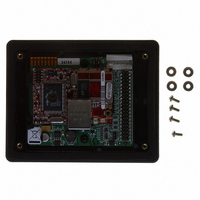
INTERFACE OP6800 W/ETHERNET PORT
Manufacturer
Rabbit Semiconductor
Datasheet
1.101-0492.pdf
(110 pages)
Specifications of 101-0492
Module/board Type
Single Board Computer Module
For Use With/related Products
SR9160
Lead Free Status / RoHS Status
Contains lead / RoHS non-compliant
Other names
316-1060


B.3 Chip Select Circuit
Figure B-1 shows a schematic of the chip select circuit located on the OP6800 module.
W
Figure B-1. Chip Select Circuit
The current drain on the battery in a battery-backed circuit must be kept at a minimum.
When the OP6800 is not powered, the battery keeps the SRAM memory contents and the
real-time clock (RTC) going. The SRAM has a powerdown mode that greatly reduces
power consumption. This powerdown mode is activated by raising the chip select (CS)
signal line. Normally the SRAM requires Vcc to operate. However, only 2 V is required
for data retention in powerdown mode. Thus, when power is removed from the circuit, the
battery voltage needs to be provided to both the SRAM power pin and to the CS signal
line. The CS control circuit accomplishes this task for the SRAM’s chip select signal line.
In a powered-up condition, the CS control circuit must allow the processor’s chip select
signal /CS1 to control the SRAM’s CS signal /CSRAM. So, with power applied, /CSRAM
must be the same signal as /CS1, and with power removed, /CSRAM must be held high
(but only needs to be battery voltage high). Q3 and Q4 are MOSFET transistors with com-
plementary polarity. They are both turned on when power is applied to the circuit. They
allow the CS signal to pass from the processor to the SRAM so that the processor can peri-
odically access the SRAM. When power is removed from the circuit, the transistors will
turn off and isolate /CSRAM from the processor. The isolated /CSRAM line has a 100 kΩ
pullup resistor to VRAM (R28). This pullup resistor keeps /CSRAM at the VRAM voltage
level (which under no power condition is the backup battery’s regulated voltage at a little
more than 2 V).
Transistors Q3 and Q4 are of opposite polarity so that a rail-to-rail voltage can be passed.
When the /CS1 voltage is low, Q3 will conduct. When the /CS1 voltage is high, Q4 con-
ducts. It takes time for the transistors to turn on, creating a propagation delay. This propa-
gation delay is typically very small, about 10 ns to 15 ns.
62
MiniCom (OP6800)
Related parts for 101-0492
Image
Part Number
Description
Manufacturer
Datasheet
Request
R

Part Number:
Description:
COMPUTER SNGLBD BL2101 A/D 0-10V
Manufacturer:
Rabbit Semiconductor
Part Number:
Description:
CARD D/A 0-10V SR9400 SMARTSTAR
Manufacturer:
Rabbit Semiconductor
Datasheet:
Part Number:
Description:
CARD A/D 0-10V SR9300 SMARTSTAR
Manufacturer:
Rabbit Semiconductor
Datasheet:

Part Number:
Description:
WiFi / 802.11 Modules & Development Tools WIRELESS CONTROL APP KIT
Manufacturer:
Rabbit Semiconductor
Part Number:
Description:
MODULE RABBITCORE RCM3720
Manufacturer:
Rabbit Semiconductor
Datasheet:
Part Number:
Description:
MODULE RABBITCORE RCM3220
Manufacturer:
Rabbit Semiconductor
Datasheet:
Part Number:
Description:
MODULE RABBITCORE RCM3210
Manufacturer:
Rabbit Semiconductor
Datasheet:
Part Number:
Description:
COMPUTER SGL-BOARD OP6600 W/SRAM
Manufacturer:
Rabbit Semiconductor
Datasheet:
Part Number:
Description:
COMPUTER SGL-BD BL2000 SRAM/FLSH
Manufacturer:
Rabbit Semiconductor
Part Number:
Description:
COMPUTER SGL-BD BL2010 SRAM/FLSH
Manufacturer:
Rabbit Semiconductor
Part Number:
Description:
COMPUTER SGL-BD BL2000 SRAM/FLSH
Manufacturer:
Rabbit Semiconductor
Part Number:
Description:
COMPUTER SGL-BD BL2020 SRAM/FLSH
Manufacturer:
Rabbit Semiconductor
Part Number:
Description:
COMPUTER SGL-BRD BL2000 MEM/FLSH
Manufacturer:
Rabbit Semiconductor
Part Number:
Description:
COMPUTER SGL-BOARD FLASH&HEADERS
Manufacturer:
Rabbit Semiconductor