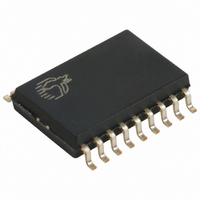
CY7C63231A-SC Cypress Semiconductor Corp, CY7C63231A-SC Datasheet - Page 17

CY7C63231A-SC
Manufacturer Part Number
CY7C63231A-SC
Description
IC MCU 3K USB LS PERIPH 18-SOIC
Manufacturer
Cypress Semiconductor Corp
Series
enCoRe™r
Datasheet
1.CY7C63231A-SXC.pdf
(50 pages)
Specifications of CY7C63231A-SC
Applications
USB Microcontroller
Core Processor
M8B
Program Memory Type
OTP (3 kB)
Controller Series
CY7C632xx
Ram Size
96 x 8
Interface
USB
Number Of I /o
10
Voltage - Supply
3.5 V ~ 5.5 V
Operating Temperature
0°C ~ 70°C
Mounting Type
Surface Mount
Package / Case
18-SOIC (7.5mm Width)
Operating Temperature (max)
70C
Operating Temperature (min)
0C
Operating Temperature Classification
Commercial
Package Type
SOIC
Mounting
Surface Mount
Lead Free Status / RoHS Status
Contains lead / RoHS non-compliant
Other names
428-1317
Available stocks
Company
Part Number
Manufacturer
Quantity
Price
Part Number:
CY7C63231A-SC
Manufacturer:
CYP
Quantity:
20 000
10.3
The Watchdog Timer Reset (WDR) occurs when the internal Watchdog timer rolls over. Writing any value to the write-only
Watchdog Reset Register at address 0x26 will clear the timer. The timer will roll over and WDR will occur if it is not cleared within
t
this event (see Section 18.0 for more details). A Watchdog Timer Reset lasts for typically 2–4 ms after which the microcontroller
begins execution at ROM address 0x0000.
11.0
The parts support a versatile low-power suspend mode. In suspend mode, only an enabled interrupt or a LOW state on the
D–/SDATA pin will wake the part. Two options are available. For lowest power, all internal circuits can be disabled, so only an
external event will resume operation. Alternatively, a low-power internal wake-up timer can be used to trigger the wake-up
interrupt. This timer is described in Section 11.2, and can be used to periodically poll the system to check for changes, such as
looking for movement in a mouse, while maintaining a low average power.
The is placed into a low-power state by setting the Suspend bit of the Processor Status and Control Register (Figure 18-1). All
logic blocks in the device are turned off except the GPIO interrupt logic, the D–/SDATA pin input receiver, and (optionally) the
wake-up timer. The clock oscillators, as well as the free-running and watchdog timers are shut down. Only the occurrence of an
enabled GPIO interrupt, wake-up interrupt, SPI slave interrupt, or a LOW state on the D–/SDATA pin will wake the part from
suspend (D– LOW indicates non-idle USB activity). Once one of these resuming conditions occurs, clocks will be restarted and
the device returns to full operation after the oscillator is stable and the selected delay period expires. This delay period is
determined by selection of internal vs. external clock, and by the state of the Ext. Clock Resume Delay as explained in Section 9.0.
In suspend mode, any enabled and pending interrupt will wake the part up. The state of the Interrupt Enable Sense bit (Bit 2,
Figure 18-1) does not have any effect. As a result, any interrupts not intended for waking from suspend should be disabled through
the Global Interrupt Enable Register and the USB End Point Interrupt Enable Register (Section 19.0).
If a resuming condition exists when the suspend bit is set, the part will still go into suspend and then awake after the appropriate
delay time. The Run bit in the Processor Status and Control Register must be set for the part to resume out of suspend.
Once the clock is stable and the delay time has expired, the microcontroller will execute the instruction following the I/O write that
placed the device into suspend mode before servicing any interrupt requests.
To achieve the lowest possible current during suspend mode, all I/O should be held at either V
bit interrupts (Figure 19-4 and Figure 19-5) should be disabled for any pins that are not being used for a wake-up interrupt. This
should be done even if the main GPIO Interrupt Enable (Figure 19-1) is off.
Typical code for entering suspend is shown below:
11.1
When exiting suspend on a wake-up event, the device can be configured to run in either Internal or External Clock mode. The
mode is selected by the state of the External Oscillator Enable bit in the Clock Configuration Register (Figure 9-2). Using the
Document #: 38-08028 Rev. *B
WATCH
...
...
...
mov a, 09h
iowr FFh
nop
...
(see Figure 10-1) of the last clear. Bit 6 (Watchdog Reset bit) of the Processor Status and Control Register is set to record
Watchdog Reset (WDR)
Clocking Mode on Wake-up from Suspend
Suspend Mode
WDR
; All GPIO set to low-power state (no floating pins, and bit interrupts disabled unless using for wake-up)
; Enable GPIO and/or wake-up timer interrupts if desired for wake-up
; Select clock mode for wake-up (see Section 11.1)
; Set suspend and run bits
; Write to Status and Control Register - Enter suspend, wait for GPIO/wake-up interrupt or USB activity
; This executes before any ISR
; Remaining code for exiting suspend routine
since last write to WDR
At least 10.1 ms
t
WATCH = 10.1 to
(at F
14.6 ms
OSC
Figure 10-1. Watchdog Reset (WDR, Address 0x26)
FOR
FOR
= 6 MHz)
WDR goes HIGH
for 2–4 ms
2–4 ms
Execution begins at
ROM Address 0x0000
CC
CY7C63221/31A
or ground. In addition, the GPIO
enCoRe™ USB
Page 17 of 50
[+] Feedback


