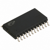
CY7C63743-SC Cypress Semiconductor Corp, CY7C63743-SC Datasheet - Page 12

CY7C63743-SC
Manufacturer Part Number
CY7C63743-SC
Description
IC MCU 8K LS USB/PS-2 24-SOIC
Manufacturer
Cypress Semiconductor Corp
Series
enCoRe™r
Specifications of CY7C63743-SC
Applications
USB Microcontroller
Core Processor
M8B
Program Memory Type
OTP (8 kB)
Controller Series
CY7C637xx
Ram Size
256 x 8
Interface
PS2, USB
Number Of I /o
16
Voltage - Supply
4 V ~ 5.5 V
Operating Temperature
0°C ~ 70°C
Mounting Type
Surface Mount
Package / Case
24-SOIC (7.5mm Width)
Lead Free Status / RoHS Status
Contains lead / RoHS non-compliant
Other names
428-1325
Available stocks
Company
Part Number
Manufacturer
Quantity
Price
Company:
Part Number:
CY7C63743-SC
Manufacturer:
CY
Quantity:
84
Company:
Part Number:
CY7C63743-SC
Manufacturer:
CYP
Quantity:
5 510
Part Number:
CY7C63743-SC
Manufacturer:
CYPRESS/赛普拉斯
Quantity:
20 000
The microcontroller begins execution from ROM address
0x0000 after a LVR, BOR, or WDR reset. Although this looks
like interrupt vector 0, there is an important difference. Reset
processing does NOT push the program counter, carry flag,
and zero flag onto program stack. Attempting to execute either
a RET or RETI in the reset handler will cause unpredictable
execution results.
The following events take place on reset. More details on the
various resets are given in the following sections.
10.1
When V
started and the Low-voltage Reset is initially enabled by
default. At the point where V
Section 25.0 for the value of V
counting for a period of t
of t
a partial suspend state to wait for V
begins executing code from address 0x0000.
As long as the LVR circuit is enabled, this reset sequence
repeats whenever the V
LVR can be disabled by firmware by setting the Low-voltage
Document #: 38-08022 Rev. *B
1. All registers are reset to their default states (all bits cleared,
2. GPIO and USB pins are set to high-impedance state.
3. The VREG pin is set to high-impedance state.
4. Interrupts are disabled.
5. USB operation is disabled and must be enabled by firmware
6. For a BOR or LVR, the external oscillator is disabled and
7. The Program Stack Pointer (PSP) and Data Stack Pointer
8. Program execution begins at address 0x0000 after the
except in Processor Status and Control Register).
if desired, as explained in Section 14.1.
Internal Clock mode is activated, followed by a time-out
period t
the clock mode, and there is no delay for V
on a WDR. Note that the External Oscillator Enable (Bit 0,
Figure 9-2) will be cleared by a WDR, but it does not take
effect until suspend mode is entered.
(DSP) reset to address 0x00. Firmware should move the
DSP for USB applications, as explained in Section 6.5.
appropriate time-out period.
START
CC
Low-voltage Reset (LVR)
). During this t
START
is first applied to the chip, the internal oscillator is
for V
WDR
CC
START
CC
since last write to WDR
START
to stabilize. A WDR does not change
At least 10.1 ms
pin voltage drops below V
time, the microcontroller enters
CC
(see Section 26.0 for the value
LVR
has risen above V
t
WATCH = 10.1 to
), an internal counter starts
(at F
14.6 ms
Figure 10-1. Watchdog Reset (WDR, Address 0x26)
CC
OSC
FOR
FOR
to stabilize before it
= 6 MHz)
CC
stabilization
LVR
LVR
. The
WDR goes HIGH
for 2–4 ms
(see
2–4 ms
Reset Disable bit in the Clock Configuration Register
(Figure 9-2). In addition, the LVR is automatically disabled in
suspend mode to save power. If the LVR was enabled before
entering suspend mode, it becomes active again once the
suspend mode ends.
When LVR is disabled during normal operation (i.e., by writing
‘0’ to the Low-voltage Reset Disable bit in the Clock Configu-
ration Register), the chip may enter an unknown state if V
drops below V
times during normal operation. If LVR is disabled (i.e., by
firmware or during suspend mode), a secondary low-voltage
monitor, BOR, becomes active, as described in the next
section. The LVR/BOR Reset bit of the Processor Status and
Control Register (Figure 20-1), is set to ‘1’ if either a LVR or
BOR has occurred.
10.2
The Brown Out Reset (BOR) circuit is always active and
behaves like the POR. BOR is asserted whenever the V
voltage to the device is below an internally defined trip voltage
of approximately 2.5V. The BOR re-enables LVR. That is, once
V
rises above V
normal operation resumes, and the microcontroller starts
executing code from address 0x00 after the t
In suspend mode, only the BOR detection is active, giving a
reset if V
is suspended and code is not executing, this lower reset
voltage is safe for retaining the state of all registers and
memory. Note that in suspend mode, LVR is disabled as
discussed in Section 10.1.
10.3
The Watchdog Timer Reset (WDR) occurs when the internal
Watchdog timer rolls over. Writing any value to the write-only
Watchdog Reset Register at address 0x26 will clear the timer.
The timer will roll over and WDR will occur if it is not cleared
within t
(Watchdog Reset bit) of the Processor Status and Control
Register is set to record this event (see Section 20.0 for more
details). A Watchdog Timer Reset typically lasts for 2–4 ms,
after which the microcontroller begins execution at ROM
address 0x0000.
CC
drops and trips BOR, the part remains in reset until V
WATCH
CC
Brown Out Reset (BOR)
Watchdog Reset (WDR)
drops below approximately 2.5V. Since the device
LVR
LVR
(see Figure 10-1) of the last clear. Bit 6
. At that point, the t
Execution begins at
ROM Address 0x0000
. Therefore, LVR should be enabled at all
START
delay occurs before
CY7C63722
CY7C63723
CY7C63743
START
Page 12 of 49
delay.
CC
CC
CC


