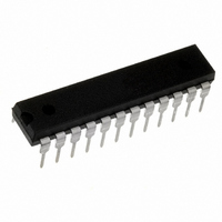
W6811IE Nuvoton Technology Corporation of America, W6811IE Datasheet - Page 12

W6811IE
Manufacturer Part Number
W6811IE
Description
IC VOICEBAND CODEC 5V/3V 24DIP
Manufacturer
Nuvoton Technology Corporation of America
Type
PCMr
Datasheet
1.W6811IE.pdf
(37 pages)
Specifications of W6811IE
Data Interface
PCM Audio Interface
Resolution (bits)
8 b
Number Of Adcs / Dacs
1 / 1
Sigma Delta
No
Voltage - Supply, Analog
4.5 V ~ 5.5 V
Voltage - Supply, Digital
2.7 V ~ 3.3 V
Operating Temperature
-40°C ~ 85°C
Mounting Type
Through Hole
Package / Case
24-DIP (0.300", 7.62mm)
For Use With
W6811DK - KIT DEVELOPMENT FOR W6811
Lead Free Status / RoHS Status
Contains lead / RoHS non-compliant
The IDL interface mode is selected when the BCLKR pin is connected to V
sync cycles. It can be used as a 2B+D timing interface in an ISDN application. The IDL interface
consists of 4 pins : IDL SYNC (FST), IDL CLK (BCLKT), IDL TX (PCMT) & IDL RX (PCMR). The FSR
pin selects channel B1 or B2 for transmit and receive. The data for channel B1 is transmitted on the
first positive edge of the IDL CLK after the IDL SYNC pulse. The IDL SYNC pulse is one IDL CLK
cycle long. The data for channel B2 is transmitted on the eleventh positive edge of the IDL CLK after
the IDL SYNC pulse. The data for channel B1 is received on the first negative edge of the IDL CLK
after the IDL SYNC pulse. The data for channel B2 is received on the eleventh negative edge of the
IDL CLK after the IDL SYNC pulse. The transmit signal pin IDL TX becomes high impedance when not
used for data transmission and also in the time slot of the unused channels. For more timing
information, see the timing section.
The system can work at 256 kHz, 512 kHz, 1536 kHz, 1544 kHz, 2048 kHz, 2560 kHz & 4096 kHz
master clock rates. The system clock is supplied through the master clock input MCLK and can be
derived from the bit-clock if desired. An internal pre-scaler is used to generate a fixed 256 kHz and an
8 kHz sample clock for the internal CODEC. The pre-scaler measures the master clock frequency
versus the Frame Sync frequency and sets the division ratio accordingly. If the Frame Sync is LOW for
the entire frame sync period while the MCLK and BCLK pin clock signals are still present, the W6811
will enter the low power standby mode. Another way to power down is to set the PUI pin to LOW.
When the system needs to be powered up again, the PUI pin needs to be set to HIGH and the Frame
Sync pulse needs to be present. It will take two Frame Sync cycles before the pin PCMT will become
low impedance.
7.4.4. Interchip Digital Link (IDL)
7.4.5. System Timing
- 12 -
Publication Release Date: September, 2005
DDD
for two or more frame
W6811
Revision A12


