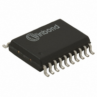
W6810ISG Nuvoton Technology Corporation of America, W6810ISG Datasheet - Page 9

W6810ISG
Manufacturer Part Number
W6810ISG
Description
IC VOICEBAND CODEC 5V 1CH 20SOP
Manufacturer
Nuvoton Technology Corporation of America
Type
PCMr
Specifications of W6810ISG
Data Interface
PCM Audio Interface
Resolution (bits)
8 b
Number Of Adcs / Dacs
1 / 1
Sigma Delta
No
Voltage - Supply, Analog
4.5 V ~ 5.5 V
Voltage - Supply, Digital
4.5 V ~ 5.5 V
Operating Temperature
-40°C ~ 85°C
Mounting Type
Surface Mount
Package / Case
20-SOP
Lead Free Status / RoHS Status
Lead free / RoHS Compliant
For Use With
W6810ES - EVALUATION SYSTEM FOR W6810W6810DK - KIT DEV/EVAL FOR W6810
Lead Free Status / RoHS Status
Compliant, Lead free / RoHS Compliant
Available stocks
Company
Part Number
Manufacturer
Quantity
Price
Part Number:
W6810ISG
Manufacturer:
NUVOTON
Quantity:
20 000
When the input amplifier is powered down, the input signal at AO or AI- needs to be referenced to the
analog ground voltage V
The output of the input amplifier is fed through a low-pass filter to prevent aliasing at the switched
capacitor 3.4 kHz low pass filter. The 3.4 kHz switched capacitor low pass filter prevents aliasing of
input signals above 4 kHz, due to the sampling at 8 kHz. The output of the 3.4 kHz low pass filter is
filtered by a high pass filter with a 200 Hz cut-off frequency. The filters are designed according to the
recommendations in the G.712 ITU-T specification. From the output of the high pass filter the signal is
digitized. The signal is converted into a compressed 8-bit digital representation with either μ-Law or A-
Law format. The μ-Law or A-Law format is pin-selectable through the μ/A-Law pin. The compression
format can be selected according to Table 7.2.
The digital 8-bit μ-Law or A-Law samples are fed to the PCM interface for serial transmission at the
sample rate supplied by the external frame sync FST.
The 8-bit digital input samples for the D-to-A path are serially shifted in by the PCM interface and
converted to parallel data bits. During every cycle of the frame sync FSR, the parallel data bits are fed
through the pin-selectable μ-Law or A-Law expander and converted to analog samples. The mode of
expansion is selected by the μ/A-Law pin as shown in Table 7.2. The analog samples are filtered by a
low-pass smoothing filter with a 3.4 kHz cut-off frequency, according to the ITU-T G.712 specification.
A sin(x)/x compensation is integrated with the low pass smoothing filter. The output of this filter is
buffered to provide the receive output signal RO-. The RO- output can be externally connected to the
PAI pin to provide a differential output with high driving capability at the PAO+ and PAO- pins. By
using external resistors (see section 11 for examples), various gain settings of this output amplifier
can be achieved. If the transmit power amplifier is not in use, it can be powered down by connecting
PAI to V
7.2. Receive Path
DD
.
AI+ (Pin 19)
V
1.2 to V
V
DD
SS
μ/A-Law Pin (Pin 16)
V
V
SS
DD
DD
AG
-1.2
.
Table 7.2. Pin-selectable Compression Format
Table 7.1 Input Amplifier Modes of operation
Input Amplifier
Powered Down
Powered Up
Powered Down
- 9 -
Format
A-Law
μ-Law
Input
AO (Pin 17)
AI+, AI- (Pins 19,18)
AI- (Pin 18)
Publication Release Date: July, 2006
W6810
Revision A13


