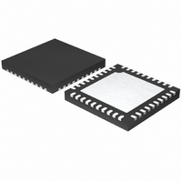
MAX9856ETL+T Maxim Integrated Products, MAX9856ETL+T Datasheet - Page 43

MAX9856ETL+T
Manufacturer Part Number
MAX9856ETL+T
Description
IC AUDIO CODEC 40TQFN-EP
Manufacturer
Maxim Integrated Products
Type
Audio Codecr
Datasheet
1.MAX9856ETL.pdf
(46 pages)
Specifications of MAX9856ETL+T
Data Interface
Serial
Resolution (bits)
18 b
Number Of Adcs / Dacs
2 / 2
Sigma Delta
Yes
S/n Ratio, Adcs / Dacs (db) Typ
77 / 91
Dynamic Range, Adcs / Dacs (db) Typ
85 / 91
Voltage - Supply, Analog
1.71 V ~ 3.6 V
Voltage - Supply, Digital
1.71 V ~ 3.6 V
Operating Temperature
-40°C ~ 85°C
Mounting Type
Surface Mount
Package / Case
40-WFQFN Exposed Pad
Lead Free Status / RoHS Status
Lead free / RoHS Compliant
Proper layout and grounding are essential for optimum
performance. Use large traces for the power-supply
inputs and amplifier outputs to minimize losses due to
parasitic trace resistance. Proper grounding improves
audio performance, minimizes crosstalk between chan-
nels, and prevents any switching noise from coupling
into the audio signal. Connect AGND, DGND, CPGND,
and PGND together at a single point on the PCB using
the star grounding technique. Route DGND, CPGND,
and all traces that carry switching transients or digital
signals separately from AGND and the analog audio
signal paths. Ground all components associated with
the charge pump to CPGND (CPVSS bypassing and
CPVDD bypassing). Connect all digital I/O termination
to DGND including DVDD and DVDDS2 bypassing.
Bypass REF and MICBIAS to AGND.
TOP VIEW
* EP = EXPOSED PAD.
JACKSNS
MICBIAS
MICGND
DVDD
DGND
AGND
MICR
MICL
INLN
INLP
31
32
33
34
35
36
37
38
39
40
30
1
29
2
______________________________________________________________________________________
+
28
PCB Layout and Bypassing
3
(6mm x 6mm)
27
4
THIN QFN
MAX9856
26
5
Pin Configuration
25
6
24 23 22
7
DirectDrive Headphone Amplifiers
*EP
8
9
10
21
Low-Power Audio CODEC with
20 CPVDD
19
18
17
16
15
14
13
12
11
C1P
CPGND
C1N
PVSS
SVSS
HPR
HPL
AVDD
HGNDSNS
Connect PVSS and SVSS together at the device and
place the charge-pump hold capacitor (C2) as close to
SVSS as possible and ground to CPGND. Bypass
CPVDD with a 1µF capacitor to CPGND and place the
bypass capacitor as close to the device as possible.
The MAX9856 thin QFN package features an exposed
thermal pad on its underside. This pad lowers the pack-
age’s thermal resistance by providing a direct heat
conduction path from the die to the PCB. Connect the
exposed thermal pad to AGND.
An evaluation kit (EV Kit) is available to provide an
example layout for the MAX9856. The EV Kit allows
quick setup of the MAX9856 and includes easy-to-use
software allowing all internal registers to be controlled.
PROCESS: BiCMOS
Chip Information
43


