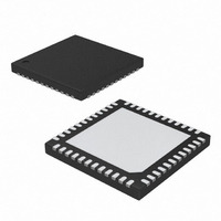
MAX9853ETM+ Maxim Integrated Products, MAX9853ETM+ Datasheet - Page 60

MAX9853ETM+
Manufacturer Part Number
MAX9853ETM+
Description
IC CODEC AUDIO STEREO 48TQFN
Manufacturer
Maxim Integrated Products
Type
Stereo Audior
Datasheet
1.MAX9851ETM.pdf
(71 pages)
Specifications of MAX9853ETM+
Data Interface
Serial
Resolution (bits)
18 b
Number Of Adcs / Dacs
2 / 2
Sigma Delta
Yes
S/n Ratio, Adcs / Dacs (db) Typ
81.5 / 88
Dynamic Range, Adcs / Dacs (db) Typ
82 / 87.5
Voltage - Supply, Analog
2.6 V ~ 3.3 V
Voltage - Supply, Digital
1.7 V ~ 3.3 V
Operating Temperature
-40°C ~ 85°C
Mounting Type
Surface Mount
Package / Case
48-TQFN Exposed Pad
Conversion Rate
48 KHz
Resolution
18 bit
Operating Supply Voltage
1.7 V to 3.3 V
Maximum Operating Temperature
+ 85 C
Mounting Style
SMD/SMT
Minimum Operating Temperature
- 40 C
Snr
75 dB
Lead Free Status / RoHS Status
Lead free / RoHS Compliant
Stereo Audio CODECs with Microphone, DirectDrive
Headphones, Speaker Amplifiers, or Line Outputs
1 = Enable.
0 = Disable.
Enable and disable the DACs only when S1SDI and
S2SDI (register 0x03 and 0x05, bit B6) are cleared and
all soft-stop sequences have completed (indicated by
the SLD bit in resister 0x00) to insure proper click-and-
pop suppression. Disable DACLEN/DACREN before
making interface mode changes.
1 = Enable.
0 = Disable.
Disable ADCLEN/ADCREN before making interface
mode changes.
1 = Enable.
0 = Disable.
VIBE goes to high impedance when the DATEN is disabled.
1 = Enable.
0 = Disable.
The MAX9851/MAX9853 feature an I
patible, 2-wire serial interface consisting of a serial data
line (SDA) and a serial clock line (SCL). SDA and SCL
Table 40. Shutdown Bit Descriptions (0x1B)
Figure 10. 2-Wire Interface Timing Diagram
SMBus is a trademark of Intel Corp.
60
REG
0x1B
______________________________________________________________________________________
Left and Right ADC Enable (ADCLEN/ADCREN)
SDA
SCL
t
HD, STA
CONDITION
Transducer/Vibe DAC Enable (DATEN)
DACLEN
START
B7
Left and Right Microphone Enable
t
LOW
Left and Right DAC Enable
DACREN
t
R
I
B6
t
2
t
SU, DAT
HIGH
C Serial Interface
(DACLEN/DACREN)
(MICLEN/MICREN)
t
F
2
C/SMBus™-com-
ADCLEN
t
HD, DAT
B5
ADCREN
t
SU, STA
B4
START CONDITION
facilitate communication between the MAX9851/
MAX9853 and the master at clock rates up to 400kHz.
Figure 10 shows the 2-wire interface timing diagram.
The master generates SCL and initiates data transfer
on the bus. A master device writes data to the
MAX9851/MAX9853 by transmitting the proper slave
address followed by the register address and then the
data word. Each transmit sequence is framed by a
START (S) or REPEATED START (Sr) condition and a
STOP (P) condition. Each word transmitted to the
MAX9851/MAX9853 is 8 bits long and is followed by an
acknowledge clock pulse. A master reading data from
the MAX9851/MAX9853 transmits the proper slave
address followed by a series of nine SCL pulses. The
MAX9851/MAX9853 transmits data on SDA in sync with
the master-generated SCL pulses. The master acknowl-
edges receipt of each byte of data. Each read
sequence is framed by a START or REPEATED START
condition, a not acknowledge, and a STOP condition.
SDA operates as both an input and an open-drain out-
put. A pullup resistor, typically greater than 500Ω, is
required on the SDA bus. SCL operates as only an
input. A pullup resistor, typically greater than 500Ω, is
required on SCL if there are multiple masters on the
bus, or if the master in a single-master system has an
open-drain SCL output. Series resistors in line with SDA
and SCL are optional. Series resistors protect the digi-
tal inputs of the MAX9851/MAX9853 from high-voltage
spikes on the bus lines, and minimize crosstalk and
undershoot of the bus signals.
REPEATED
DATEN
t
HD, STA
B3
Shutdown Control Register (0x1B)
B2
t
SP
0
t
SU, STO
MICLEN
CONDITION
STOP
B1
t
BUF
CONDITION
START
MICREN
B0


