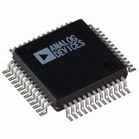
AD1835AS Analog Devices Inc, AD1835AS Datasheet

AD1835AS
Specifications of AD1835AS
Related parts for AD1835AS
AD1835AS Summary of contents
Page 1
FEATURES 5 V Stereo Audio System with 3.3 V Tolerant Digital Interface Supports kHz Sample Rates 192 kHz Sample Rate Available on One DAC Supports 16-/20-/24-Bit Word Lengths Multibit - Modulators with Perfect Differential Linearity Restoration for ...
Page 2
AD1835–SPECIFICATIONS TEST CONDITIONS Supply Voltages (AVDD, DVDD) 5.0 V Ambient Temperature 25°C 12.288 MHz (256 × f Input Clock ADC Input Signal 1.0078125 kHz, –1 dBFS (Full Scale) DAC Input Signal 1.0078125 kHz, 0 dBFS (Full Scale) Input Sample Rate ...
Page 3
Parameter ADC DECIMATION FILTER, 96 kHz* Pass Band Pass-Band Ripple Stop Band Stop-Band Attenuation Group Delay DAC INTERPOLATION FILTER, 48 kHz* Pass Band Pass-Band Ripple Stop Band Stop-Band Attenuation Group Delay DAC INTERPOLATION FILTER, 96 kHz* Pass Band Pass-Band Ripple ...
Page 4
AD1835 TIMING SPECIFICATIONS Parameter MASTER CLOCK AND RESET t MCLK High MH t MCLK Low ML PD/RST Low t PDR SPI PORT t CCLK High CCH t CCLK Low CCL t CCLK Period CCP t CDATA Setup CDS t CDATA ...
Page 5
Parameter TDM256 MODE (Master) t BCLK Delay TBD t FSTDM Delay FSD t ASDATA Delay TABDD t DSDATA1 Setup TDDS t DSDATA1 Hold TDDH TDM256 MODE (Slave) f BCLK Frequency AB t BCLK High TBCH t BCLK Low TBCL t ...
Page 6
... Exposure to absolute maximum rating conditions for extended periods may affect device reliability. Model AD1835AS AD1835AS-REEL EVAL-AD1835EB CAUTION ESD (electrostatic discharge) sensitive device. Electrostatic charges as high as 4000 V readily accumulate on the human body and test equipment and can discharge without detection. Although the AD1835 features proprietary ESD protection circuitry, permanent damage may occur on devices subjected to high energy electrostatic discharges ...
Page 7
DVDD CLATCH CIN PD/RST AGND OUTLN1 OUTLP1 OUTRN1 OUTRP1 AGND AVDD OUTLN2 OUTLP2 Pin No. Mnemonic 1, 39 DVDD 2 CLATCH 3 CIN PD/RST 4 5, 10, 16, 24, 30, 35 AGND 6, 12, 25, 31 OUTLNx 7, 13, 26, ...
Page 8
AD1835–Typical Performance Characteristics 0 –50 –100 –150 0 5 FREQUENCY (Normalized to TPC 1. ADC Composite Filter Response 5 0 –5 –10 –15 –20 –25 – FREQUENCY (Hz) TPC 2. ADC High-Pass Filter Response –50 ...
Page 9
FREQUENCY (kHz) TPC 7. DAC Composite Filter Response, f 0.10 0.05 0 –0.05 –0. FREQUENCY (kHz) TPC 8. DAC Composite Filter Response, f (Pass-Band Section) REV. B 0.2 0.1 0 ...
Page 10
AD1835 TERMINOLOGY Dynamic Range The ratio of a full-scale input signal to the integrated input noise in the pass band ( kHz), expressed in decibels (dB). Dynamic range is measured with a –60 dB input signal and ...
Page 11
FUNCTIONAL OVERVIEW ADCs There are two ADC channels in the AD1835, configured as a stereo pair. Each ADC has fully differential inputs. The ADC section can operate at a sample rate kHz. The ADCs include on-board ...
Page 12
AD1835 To maintain the highest performance possible recommended that the clock jitter of the master clock signal be limited to less than 300 ps rms, measured using the edge-to-edge technique. Even at these levels, extra noise or tones ...
Page 13
CLS t CLATCH CCP CCLK CIN D15 D14 t COE COUT LRCLK LEFT CHANNEL BCLK SDATA MSB LEFT CHANNEL LRCLK BCLK MSB SDATA LEFT CHANNEL LRCLK BCLK MSB SDATA LRCLK BCLK SDATA MSB NOTES 1. DSP MODE DOES NOT ...
Page 14
AD1835 t ABH ABCLK t ABL t ALS ALRCLK ASDATA LEFT-JUSTIFIED MSB MODE ASDATA MODE ASDATA RIGHT-JUSTIFIED MODE t DBH DBCLK t DBL t DLS DLRCLK t DDS DSDATA LEFT-JUSTIFIED MSB MODE t DDH DSDATA 2 I ...
Page 15
LRCLK BCLK ADC DATA LRCLK BCLK DAC DATA t t ABH ABP ABCLK t ABL t ALS ALRCLK t ALH t ADS ASDATA MSB t ADH Figure 9. ADC Packed Mode Timing REV. B 256 BCLKs 32 BCLKs SLOT 1 ...
Page 16
AD1835 2 Pin Name I 2 ASDATA ( DSDATA1 ( DSDATA2 (I)/AAUXDATA1 ( DSDATA3 (I)/AAUXDATA2 ( DSDATA4 (I)/AAUXDATA3 (I) I ALRCLK (O) LRCLK for ADC ABCLK (O) BCLK for ADC DLRCLK (I)/AUXLRCLK(I/O) ...
Page 17
LRCLK BCLK ADC 1 SLAVE DATA MCLK LRCLK BCLK ADC 1 SLAVE DATA MCLK LRCLK BCLK ADC 2 SLAVE DATA MCLK Figure 12. Aux Mode Connection to SHARC (Master Mode) LRCLK BCLK ADC 1 MASTER DATA MCLK LRCLK BCLK ADC ...
Page 18
AD1835 CONTROL/STATUS REGISTERS The AD1835 has 15 control registers which are used to set the operating mode of the part. The other two registers, ADC Peak 0 and ADC Peak 1, are read-only and should not be programmed. ...
Page 19
Register Register Address Name 0000 DACCTRL1 0001 DACCTRL2 0010 DACVOL1 0011 DACVOL2 0100 DACVOL3 0101 DACVOL4 0110 DACVOL5 0111 DACVOL6 1000 DACVOL7 1001 DACVOL8 1010 ADCPeak0 1011 ADCPeak1 1100 ADCCTRL1 1101 ADCCTRL2 1110 ADCCTRL3 1111 Reserved Address R/W RES De-Emphasis ...
Page 20
AD1835 Table VI. DAC Volume Control Address R/W RES DAC Volume 15, 14, 13 0010 = DACL1 0 0 0000000000 = 1/1024 0011 = DACR1 0000000001 = ...
Page 21
F 600Z 5.76k 5.76k AUDIO + INPUT 120pF NPO 100pF NPO OP275 V REF 5.76k 5.76k 750k OP275 V REF Figure 14. Typical ADC Input Filter Circuit REV. B 237 OUTLNx ADCxN 1nF NPO 100pF NPO OUTLPx 1nF NPO ...
Page 22
AD1835 SEATING PLANE VIEW A OUTLINE DIMENSIONS 52-Lead Metric Quad Flat Package [MQFP] (S-52) Dimensions shown in millimeters 13.45 1.03 13.20 SQ 2.45 0.88 12.95 MAX 0. 7.80 TOP VIEW REF (PINS DOWN) PIN 0.23 ...
Page 23
Revision History Location 7/03—Data Sheet changed from REV REV. B. Changes to SPECIFICATIONS . . . . . . . . . . . . . . . . . . . . . . . . . ...
Page 24
–24– ...


