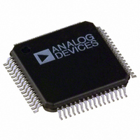
ADV7202KST Analog Devices Inc, ADV7202KST Datasheet - Page 19

ADV7202KST
Manufacturer Part Number
ADV7202KST
Description
IC CODEC VIDEO 10BIT 64LQFP
Manufacturer
Analog Devices Inc
Type
Video Codecr
Datasheet
1.ADV7202KSTZ.pdf
(28 pages)
Specifications of ADV7202KST
Rohs Status
RoHS non-compliant
Data Interface
Serial
Resolution (bits)
12, 10 b
Number Of Adcs / Dacs
1 / 4
Sigma Delta
No
Voltage - Supply, Analog
4.75 V ~ 5.25 V
Voltage - Supply, Digital
4.75 V ~ 5.25 V
Operating Temperature
0°C ~ 70°C
Mounting Type
Surface Mount
Package / Case
64-LQFP
Lead Free Status / Rohs Status
Not Compliant
Available stocks
Company
Part Number
Manufacturer
Quantity
Price
Company:
Part Number:
ADV7202KST
Manufacturer:
CSR
Quantity:
1 000
Company:
Part Number:
ADV7202KSTZ
Manufacturer:
Analog Devices Inc
Quantity:
10 000
REV. 0
CLAMP REGISTER 0
CR0 (CR00–CR07)
(Address (SR4–SR0) = 06H)
Figure 21 shows the various operations under the control of
Clamp Register 0.
CR0 BIT DESCRIPTION
Clamp Level/16 (CR00–CR06)
To perform an accurate AGC gain operation, it is necessary
to know to what level the user is clamping the black level. This
black level is then subtracted from the 10-bit ADC output
before gaining. It is then added on again afterwards. It should
be noted that this register is seven bit and will hold the value of
Clamp Value/16.
Reserved (CR07)
Zero must be written to this bit.
CLAMP REGISTER 1
CR1 (CR10–CR17)
(Address (SR4–SR0) = 07H)
Figure 22 shows the various operations under the control of
Clamp Register 1.
ZERO MUST BE
WRITTEN TO
THIS BIT
CR17
CR17
CR16
0
1
SYNCHRONIZE
ZERO MUST BE
WRITTEN TO
THIS BIT
CLAMPS
OFF
ON
CR07
CR07
CR16
CR06
CR15
CR15 CR14 CR13
0
0
0
0
1
1
1
1
0
0
1
1
0
0
1
1
COARSE CLAMP ON TIME
Figure 21. Clamp Register 0
Figure 22. Clamp Register 1
CR05
CR14
0
1
0
1
0
1
0
1
7-BIT [6:0] CLAMP LEVEL,
CR00 HOLDS THE LSB,
CR06 THE MSB
CR04
2 CLOCK CYCLES
4 CLOCK CYCLES
8 CLOCK CYCLES
16 CLOCK CYCLES
32 CLOCK CYCLES
64 CLOCK CYCLES
128 CLOCK CYCLES
256 CLOCK CYCLES
CR13
CLAMP LEVEL
CR06–CR00
–19–
CR1 BIT DESCRIPTION
Fine Clamp On Time (CR10–CR12)
There are three fine clamp circuits on the chip. This word
controls the number of clock cycles for which the fine clamps
are switched on per video line. The clamp is switched on after a
SYNC pulse is received on the SYNC_IN pin, provided the
relevant enabling bit is set (see CR16).
Coarse Clamp On Time (CR13–CR15)
There are three coarse clamp circuits on the chip. This I
word controls the number of clock cycles for which the fine
clamps are switched on per video line. The clamp is switched on
after a SYNC pulse is received on the SYNC_IN pin, provided
the relevant enabling bit is set (see CR16).
Synchronize Clamps (CR16)
Setting this bit to “1” forces the clamps to wait until the next
sync pulse before switching on.
Reserved (CR17)
Zero must be written to this bit.
CR03
CR12
CR02
CR11
CR12 CR11 CR10
0
0
0
0
1
1
1
1
0
0
1
1
0
0
1
1
FINE CLAMP ON TIME
CR01
CR10
0
1
0
1
0
1
0
1
2 CLOCK CYCLES
4 CLOCK CYCLES
8 CLOCK CYCLES
16 CLOCK CYCLES
32 CLOCK CYCLES
64 CLOCK CYCLES
128 CLOCK CYCLES
256 CLOCK CYCLES
CR00
ADV7202
2
C


