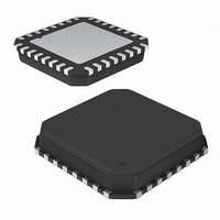
CY7C63833-LTXC Cypress Semiconductor Corp, CY7C63833-LTXC Datasheet - Page 34

CY7C63833-LTXC
Manufacturer Part Number
CY7C63833-LTXC
Description
IC USB PERIPHERAL CTRLR 32VQFN
Manufacturer
Cypress Semiconductor Corp
Series
CY7Cr
Type
USB Peripheral Controllerr
Datasheet
1.CY7C63310-SXC.pdf
(86 pages)
Specifications of CY7C63833-LTXC
Package / Case
32-VQFN Exposed Pad, 32-HVQFN, 32-SQFN, 32-DHVQFN
Controller Type
USB Peripheral Controller
Interface
USB
Voltage - Supply
4 V ~ 5.5 V
Current - Supply
40mA
Operating Temperature
0°C ~ 70°C
Mounting Type
Surface Mount
Mounting Style
SMD/SMT
Operating Temperature Range
0 C to + 70 C
Supply Current
40 mA
Operating Supply Voltage
4 V to 5.5 V
Lead Free Status / RoHS Status
Lead free / RoHS Compliant
For Use With
770-1001 - ISP 4PORT CYPRESS ENCORE II MCUCY4623 - KIT MOUSE REFERENCE DESIGN428-1774 - EXTENSION KIT FOR ENCORE II428-1773 - KIT DEVELOPMENT ENCORE II
Lead Free Status / Rohs Status
Lead free / RoHS Compliant
Available stocks
Company
Part Number
Manufacturer
Quantity
Price
Company:
Part Number:
CY7C63833-LTXC
Manufacturer:
Cypress
Quantity:
2 814
Part Number:
CY7C63833-LTXC
Manufacturer:
CYPRESS/赛普拉斯
Quantity:
20 000
14. General Purpose I/O (GPIO) Ports
14.1 Port Data Registers
Table 14-1. P0 Data Register (P0DATA)[0x00] [R/W]
Document 38-08035 Rev. *N
This register contains the data for Port 0. Writing to this register sets the bit values to be output on output enabled pins. Reading
from this register returns the current state of the Port 0 pins.
Bit 7: P0.7 Data
P0.7 only exists in the CY7C638xx
Bit [6:5]: P0.6–P0.5 Data/TIO1 and TIO0
Besides their use as the P0.6–P0.5 GPIOs, these pins are also used for the alternate functions as the Capture Timer input or
Timer output pins (TIO1 and TIO0). To configure the P0.5 and P0.6 pins, refer to the P0.5/TIO0–P0.6/TIO1 Configuration Register
(Table 14-4 on page
The use of the pins as the P0.6–P0.5 GPIOs and the alternate functions exist in all the enCoRe II parts.
Bit [4:2]: P0.4–P0.2 Data/INT2 – INT0
Besides their use as the P0.4–P0.2 GPIOs, these pins are also used for the alternate functions as the Interrupt pins (INT0–INT2).
To configure the P0.4–P0.2 pins, refer to the P0.2/INT0–P0.4/INT2 Configuration Register
The use of the pins as the P0.4–P0.2 GPIOs and the alternate functions exist in all the enCoRe II parts.
Bit 1: P0.1/CLKOUT
Besides its use as the P0.1 GPIO, this pin is also used for an alternate function as the CLK OUT pin. To configure the P0.1 pin,
refer to the P0.1/CLKOUT Configuration Register
Bit 0: P0.0/CLKIN
Besides its use as the P0.0 GPIO, this pin is also used for an alternate function as the CLKIN pin. To configure the P0.0 pin,
refer to the P0.0/CLKIN Configuration Register
Read/Write
Default
Field
Bit #
P0.7
R/W
7
0
38).
P0.6/TIO1
R/W
6
0
P0.5/TIO0
R/W
(Table 14-1 on page
5
0
(Table 14-2 on page
P0.4/INT2
R/W
4
0
37).
37).
P0.3/INT1
R/W
3
0
P0.2/INT0
R/W
CY7C63310, CY7C638xx
(Table 14-3 on page
2
0
P0.1/CLKOUT
R/W
1
0
38).
P0.0/CLKIN
Page 34 of 86
R/W
0
0
[+] Feedback


